Light-emitting device having semiconductor nanocrystal complexes

a technology of semiconductor nanocrystals and light-emitting devices, which is applied in semiconductor devices, semiconductor/solid-state device details, electrical devices, etc., can solve the problems of reducing efficiency of “warm white” leds made from a combination of yellow and red, affecting the display of red matter, and affecting the appearance of red matter

Active Publication Date: 2008-10-09
SAMSUNG ELECTRONICS CO LTD
View PDF5 Cites 110 Cited by
  • Summary
  • Abstract
  • Description
  • Claims
  • Application Information

AI Technical Summary

Benefits of technology

[0013]Devices according to embodiments of the invention may include a light source typically having a peak emission wavelength between 450 nm and 480 nm, an active layer disposed over the light-emitting diode chip, and one or more populations of semiconductor nanocrystals disposed within the active layer, where the semiconductor nanocrys

Problems solved by technology

However “warm white” LEDs made from a combination of yellow and red have reduced efficiency owing to the lower quantum yield of the red phosphors and also because the red phosphors are broadband emitters.
A second problem associated with traditional white-light LEDs comprising 450-470 nm blue LEDs with a broadband yellow YAG:Ce phosphor is that often the “red”, “green”, or “blue” portions of the emitted spectrum light does not adequately match the spectrum of a true white blackbody spectrum.
This leads to a problem that a matter to be displayed in red looks subdued.
This problem is often referred to as poor color rendering.
If the individual chips are located close to one ano

Method used


Image

  • Light-emitting device having semiconductor nanocrystal complexes
  • Light-emitting device having semiconductor nanocrystal complexes
  • Light-emitting device having semiconductor nanocrystal complexes

Examples


examples

[0088]Specific representative examples will now be described, including how such examples were prepared. It is understood that the specific methods, materials, conditions, process parameters, apparatus and the like are non-limiting.

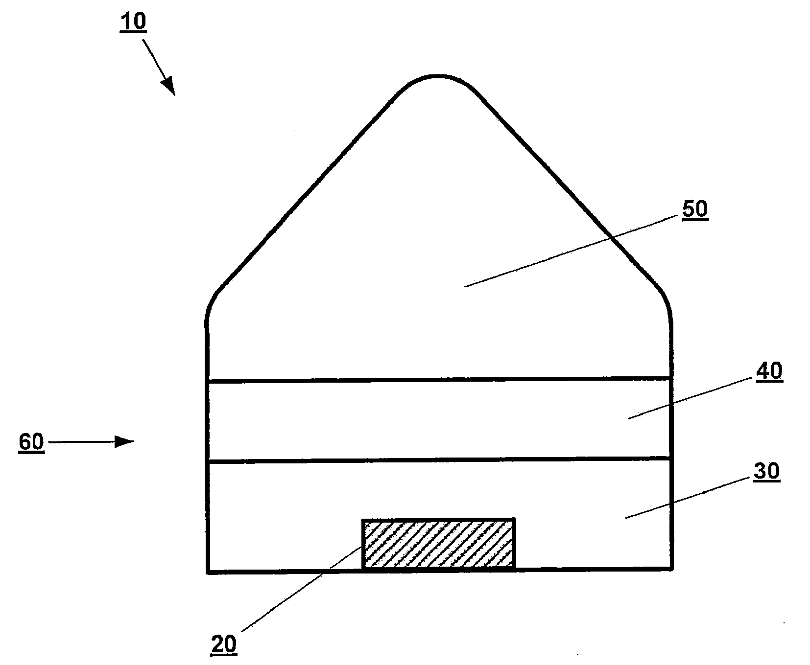
[0089]Various Active Layer Locations on the LED

[0090]Devices according to embodiments of the present invention may be fabricated on low power SMD-type LEDs, such as those available commercially from Cree, Optosupply, and Knowledge-On Inc.). To place a semiconductor nanocrystal layer in various locations, different volumes of matrix for a first encapsulant layer were deposited on blue light emitting LEDs. Three test devices were prepared with volumes for the first encapsulant layer of 0, 1.4, and 2.1 μL for devices 1, 2, and 3, respectively. Each 1 μL can make thickness in the range of 0.1-1 mm, which is dependant on the LED size, type and form factors. The Knowledge-On LED has the form factors with 2.4 mm in diameter and about 1 mm in depth, and surrounde...


PUM


Abstract

Light-emitting devices are provided that incorporate one or more underlying LED chips or other light sources and a layer having one or more populations of nanoparticles disposed over the light source. The nanoparticles may absorb some light emitted by the underlying source, and re-emit light at a different level. By varying the type and relative concentration of nanoparticles, different emission spectra may be achieved. White light and specialty-color emission may be achieved. Devices also may include multiple LED chips, with nanoparticles disposed over one or more underlying chips in an array.

Description

RELATED APPLICATIONS[0001]This application claims the benefit of U.S. Provisional Application No. 60 / 873,532, filed Dec. 8, 2006, and U.S. Provisional Application No. 60 / 875,604, filed Dec. 19, 2006, each of which is incorporated herein by reference in its entirety.BACKGROUND[0002]Semiconductor nanocrystals are tiny crystals typically made of II-VI, III-V, IV-VI, and I-III-VI semiconductor materials that have a diameter between 1 nanometer (nm) and 20 nm. In the strong confinement limit, the physical diameter of the nanocrystal is smaller than the bulk excitation Bohr radius causing quantum confinement effects to predominate. In this regime, the nanocrystal is a 0-dimensional system that has both quantized density and energy of electronic states where the actual energy and energy differences between electronic states are a function of both the nanocrystal composition and physical size. Larger nanocrystals have more closely spaced energy states and smaller nanocrystals have the rever...

Claims


Application Information

Patent Timeline
IPC IPC(8): H01L33/00H01L33/50
CPCB82Y20/00H01L33/502
Inventor GILLIES, JENNIFERSOCHA, DAVIDCHEON, KWANG OHKLOCASIO, MICHAEL
Owner SAMSUNG ELECTRONICS CO LTD
Why Eureka
Try Eureka