Multi-Operation Write Aggregator Using a Page Buffer and a Scratch Flash Block in Each of Multiple Channels of a Large Array of Flash Memory to Reduce Block Wear

a multi-operation write and scratch flash technology, applied in the field of flash memory systems, can solve the problems of mlc flash performance, flash wearout and unreliability, and limitations of nand flash, and achieve the effect of reducing performance, reliability and durability of mlc flash

Inactive Publication Date: 2008-10-09
SUPER TALENT TECH CORP
View PDF6 Cites 179 Cited by
  • Summary
  • Abstract
  • Description
  • Claims
  • Application Information

AI Technical Summary

Problems solved by technology

However, NAND flash has limitations.
One limitation of NAND flash is that when storing data (writing to flash), the flash can only write from ones (1) to zeros (0).
Another limitation is that NAND flash memory has a finite number of erase cycles between 10,000 to 1,000,000, after which the flash wear out and becomes unreliable.
But the performance, reliability and durability may decrease for MLC flash.
But it has a lower write speed than SLC flash memory, which means that it takes a longer time to store pictures when taking snapshots.
Its low performance requires a stronger wear-leveling algorithm to meet consumers' needs.
In addition, the life of MLC flash memory is limited to perhaps 10,000 erase cycles.
However, the size of the host data being stored is not expected to increase at the same rate as the block size.
Thus flash blocks are less efficiently used as the flash blocks become larger, but store fixed-size pieces of host data.
However, moving data around among flash blocks increases wear, as flash blocks need to be erased.
Paging and disk de-fragmenting methods, which have been used for main DRAM memories and hard disks, are ineffective for flash memory due to the restricted life of flash.
Such methods would quickly wear out the flash memory blocks.
A large DRAM or SRAM buffer could be used to merge writes before writing to flash, but if power is lost, the data in the write buffer may also be lost.
The size of the write buffer may be prohibitive, especially as flash blocks increase in size, since the write buffer needs to have a size equal to one or more flash blocks.
However, moving data from one channel to another during wear-leveling may decrease performance.

Method used


Image

  • Multi-Operation Write Aggregator Using a Page Buffer and a Scratch Flash Block in Each of Multiple Channels of a Large Array of Flash Memory to Reduce Block Wear
  • Multi-Operation Write Aggregator Using a Page Buffer and a Scratch Flash Block in Each of Multiple Channels of a Large Array of Flash Memory to Reduce Block Wear
  • Multi-Operation Write Aggregator Using a Page Buffer and a Scratch Flash Block in Each of Multiple Channels of a Large Array of Flash Memory to Reduce Block Wear

Examples


example a

[0114]Assume that six AFB blocks do not store valid data. Moreover, the host transmits data in a sequence of three sectors, two sectors, and one sector, separately, to the flash system using three write requests with different target addresses.

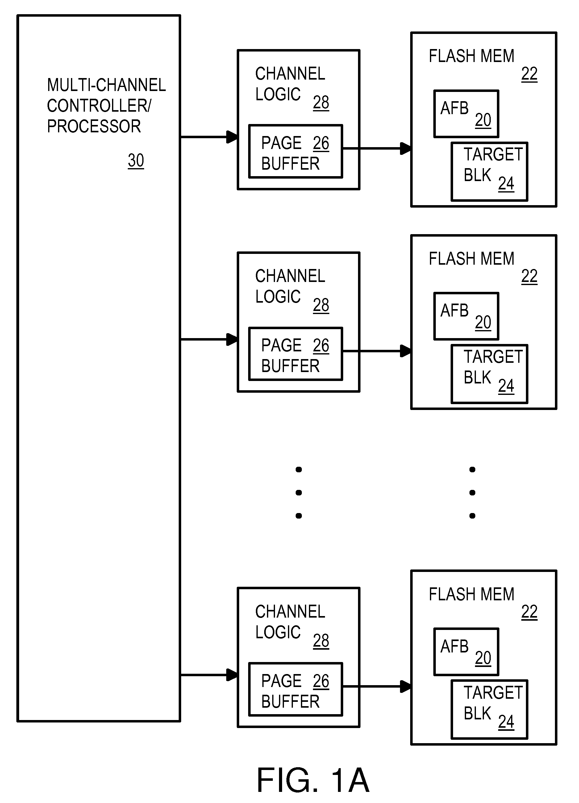
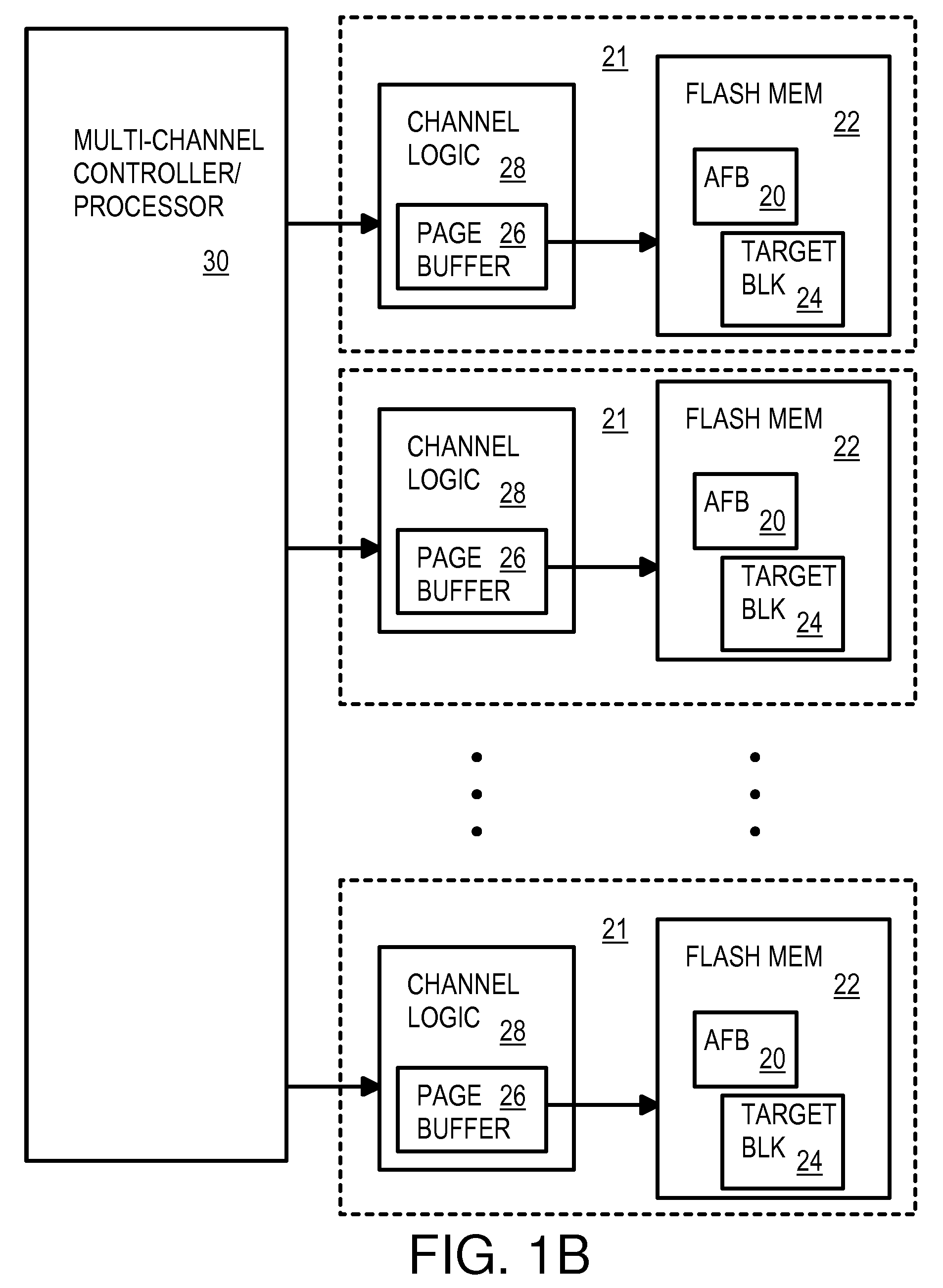
[0115]FIG. 11A shows channel A being used to send host data in page buffer A of multi-page buffer 314 to AFB block #1, the first entry in AFB tracking table 350. Channel B is being used to copy host data in page buffer B to AFB block #2, and channel C is being used to copy host data in page buffer C to AFB block #3.

[0116]FIG. 11B shows the timing where host data is accumulated into page buffer A then copied to AFB #1. Host data from the second transaction is accumulated to page buffer B and then copied over channel B to AFB #2, and host data from the third transaction is accumulated to page buffer C and then copied over channel C to AFB #3.

[0117]FIGS. 12A-D show the AFB tracking table for the example of FIGS. 11A-B. AFB tracking table 350 has ...

example c

[0131]FIGS. 13A-B show the AFB tracking table for example C and FIGS. 14A-B.

[0132]Assume that six AFB blocks have stored valid data, as shown in FIG. 13A. The host sends a write request to the device with a target address=0111—0000. The current writing address does not match the target LSA of any AFB block in AFB tracking table 350.

[0133]Step 1: Receive a write request. The Multiple AFB Block Management sets CDF=1 and AMF=0. Receive two data sectors from the host, and write the sectors sequentially in Buffer A through Channel A.

[0134]Step 2: Start the flow chart of FIG. 9 to search for an available AFB block to copy the page buffer data into. FIG. 13A shows that all of the AFB blocks have stored valid data; none are empty and available.

[0135]Step 3: Duplicate the valid data stored in AFB Block 1 to the corresponding page of the target physical block.

[0136]Step 4: Remove the entry of AFB Block 1. (Details are shown in FIG. 10)

[0137]Step 5: Assign an available physical block to be AFB...

example d

[0142]FIGS. 15A-B show the AFB tracking table for example D. Assume that three AFB blocks have stored valid data, as shown in FIG. 15A. In this example, the entry of AFB Block 3 needs to be removed from AFB tracking table 350.

[0143]Step 1: Start the flow chart of FIG. 10 to remove the third entry of AFB tracking table 350. (k=3 and N=6)

[0144]Step 2: Set bank_num=1034 and page_num=11.

[0145]Step 3: Duplicate the entry of AFB Block 4 to that of Block 3.

[0146]Step 4: Duplicate the entry of AFB Block 5 to that of Block 4.

[0147]Step 5: Duplicate the entry of AFB Block 6 to that of Block 5.

[0148]Step 6: Modify the entry of AFB Block 6 to change the physical block number and last page number to bank_num and page_num, respectively. Moreover, set the valid data flag to be zero. Finally, the modified AFB tracking table is shown in FIG. 15B.

[0149]After removing the entry of AFB Block 3, the order of available AFB blocks is assigned numbers 3 to 6. Note that the previously removed AFB block is t...


PUM


Abstract

A flash system has multiple channels of flash memory chips that can be accessed in parallel. Host data is assigned to one of the channels by a multi-channel controller processor and accumulated in a multi-channel page buffer. When a page boundary in the page buffer is reached, the page buffer is written to a target physical block if full, or combined with old data fragments in an Aggregating Flash Block (AFB) when the logical-sector addresses (LSA's) match. Thus small fragments are aggregated using the AFB, reducing erases and wear of flash blocks. The page buffer is copied to the AFB when a STOP command occurs. Each channel has one or more AFB's, which are tracked by an AFB tracking table.

Description

RELATED APPLICATION[0001]This application is a continuation-in-part (CIP) of U.S. patent application for “High Integration of Intelligent Non-Volatile Memory Devices”, Ser. No. 12 / 054,310, filed Mar. 24, 2008, which is a CIP of “High Endurance Non-Volatile Memory Devices”, Ser. No. 12 / 035,398, filed Feb. 21, 2008, which is a CIP of “High Speed Controller for Phase Change Memory Peripheral Devices”, U.S. application Ser. No. 11 / 770,642, filed on Jun. 28, 2007, which is a CIP of “Local Bank Write Buffers for Acceleration a Phase Change Memory”, U.S. application Ser. No. 11 / 748,595, filed May 15, 2007, which is CIP of “Flash Memory System with a High Speed Flash Controller”, application Ser. No. 10 / 818,653, filed Apr. 5, 2004, now U.S. Pat. No. 7,243,185.[0002]This application is also a CIP of co-pending U.S. patent Application for “Method and Systems of Managing Memory Addresses in a Large Capacity Multi-Level Cell (MLC) based Memory Device”, Ser. No. 12 / 025,706, filed on Feb. 4, 2008...

Claims


Application Information

Patent Timeline
Patent Type & Authority Applications(United States)
IPC IPC(8): G06F12/02
CPCG06F12/0246G06F21/32G06F21/78G06F2212/1036G06F2212/7202G06F2212/7208G06K19/07G06K19/07354
Inventor CHOW, DAVID Q.YU, FRANKLEE, CHARLES C.MA, ABRAHAM C.SHEN, MING-SHIANG
Owner SUPER TALENT TECH CORP
Why Eureka
Try Eureka