Rfid Tag, Method For Manufacturing Rfid Tag and Method For Arranging Rfid Tag

a technology of rfid tags and tags, applied in the field of rfid tags, can solve the problems of enlargement of the size of the active type tag, high cost, and impossibility of mounting locations, and achieve the effect of more stable long-distance radio communication and increased flexibility of mounting locations

Inactive Publication Date: 2008-10-16
MITSUBISHI ELECTRIC CORP
View PDF14 Cites 43 Cited by
  • Summary
  • Abstract
  • Description
  • Claims
  • Application Information

AI Technical Summary

Benefits of technology

[0068]As a result, while the flexibility of the mounting location can be increased as compared with conventional RFID tags, there is prov

Problems solved by technology

While active-type tags have merits, such as a long communication range and communicative stability, as compared with passive-type tags, because they include a battery therein, active-type tags also have demerits, such as complication in their structure, enlargement of their size, and high cost.
In the case of an RFID tag which operates in a high frequency band, such as a UHF band or a microwave band, because a radio frequency communication method is applied, and power is furnished to the IC chip of the RFID tag using an electric wave, its communication range is improved greatly and reaches about 1 to 8 m. Therefore, an RFID system having this type of RFID tags can carry out batch reading of a plurality of RFID tags, reading of a moving RFID tag, and so on, which are difficult for an RFID system having a short communication range and operating in a low frequency band or a short frequency band to carry out, and it can be therefore expected that the use of the RFID system is spread greatly among a wide of fields.
Because a conventional RFID tag (an RFID tag disclosed by patent reference 1) is constructed as mentioned above, there is a problem that in a case in which an RFID tug is attached to a conductive object (a conductor), such as a metallic object, or is mounted in the vicinity of an conductive object, the dipole antenna 1 of the tug stops operating under the influence of the conductive object, and its communication range becomes short extremely.
Although it is possible to mount an RFID tag disclosed by patent reference 2 to a metallic object (a conductor), there is a problem that the structure of the tag becomes complicated and therefore manufacturing the tag becomes difficult, and this results in increase in the manufacturing cost because the RFID tag is constructed in such a manner that an IC chip is connected between a ½-wave microstrip line resonator and a ground conductor plate and it is therefore necessary to embed the IC chip into a dielectric substrate.
More specifically, there is a problem that when the antenna pattern and the IC chip are mounted in the substrate, there is a possibility that the IC chip might be damaged by a shock or the like, and it becomes difficult to print something directly on the surface (the

Method used


Image

  • Rfid Tag, Method For Manufacturing Rfid Tag and Method For Arranging Rfid Tag
  • Rfid Tag, Method For Manufacturing Rfid Tag and Method For Arranging Rfid Tag
  • Rfid Tag, Method For Manufacturing Rfid Tag and Method For Arranging Rfid Tag

Examples


embodiment 1

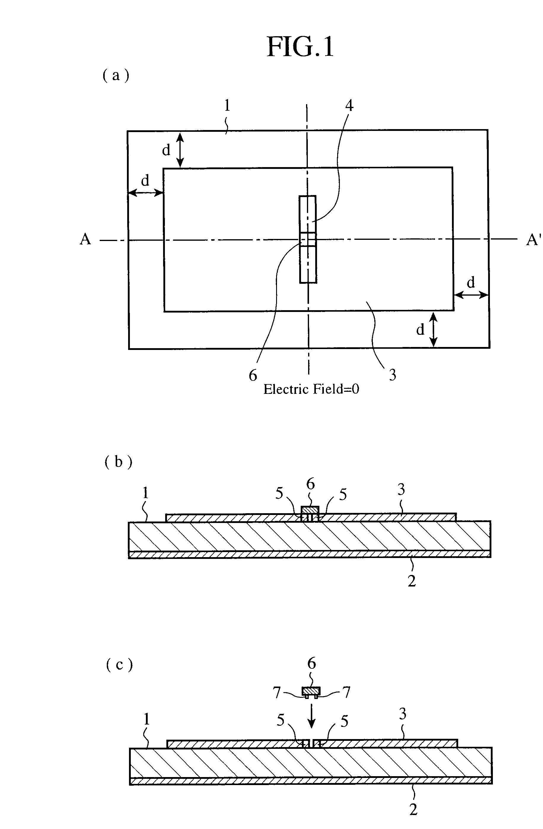
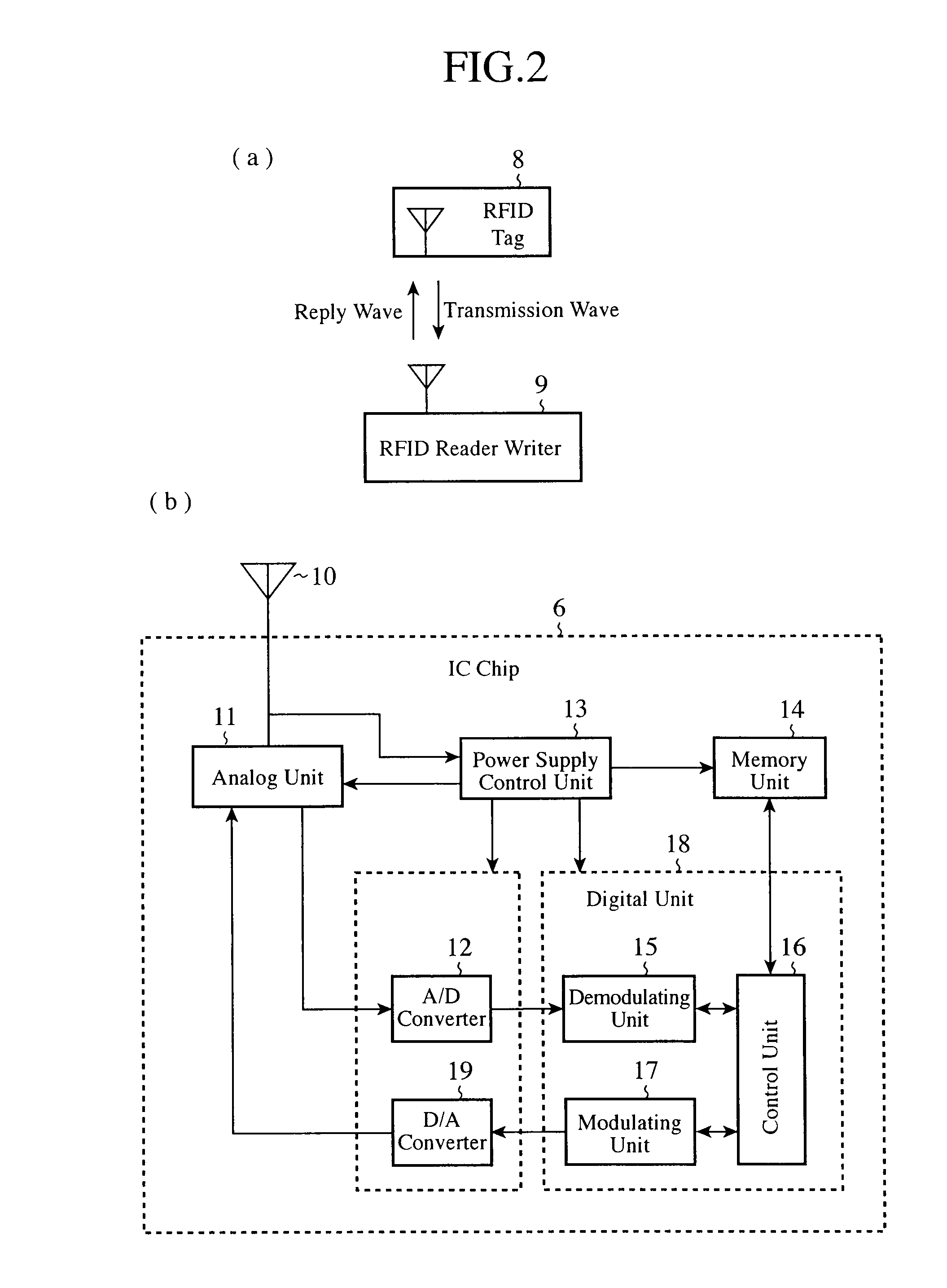
[0121]Hereafter, Embodiment 1 of the present invention will be explained with reference to FIGS. 1 to 6. FIG. 1 is a structural diagram of an RFID tag in accordance with Embodiment 1, FIG. 1(a) is a surface view of a dielectric substrate, FIG. 1(b) is a partially sectional view 1 of the dielectric substrate taken along the line A-A′, FIG. 1(c) is a partially sectional view 2 of the dielectric substrate taken along the line A-A′, FIG. 2 is a basic block diagram of an RFID system, FIG. 2(a) is a diagram of the RFID system, FIG. 2(b) is a functional block diagram of the RFID tag, FIG. 3 is a graphical representation of an electric field of the RFID tag, FIG. 4 is a drawing of the characteristic impedance of the RFID tag in accordance with Embodiment 1, FIG. 5 is a drawing showing that electrical connecting portions of the RFID tag in accordance with Embodiment 1 of the present invention are exposed, FIG. 5(a) is a drawing of a 2-terminal example of the RFID tag, FIG. 5(b) is a drawing ...

embodiment 2

[0128]Embodiment 2 of the present invention will be explained with reference to FIGS. 7 to 10. FIG. 7 is a structural diagram of an RFID tag in accordance with Embodiment 2, FIG. 8 is a structural diagram of an RFID tag in accordance with Embodiment 2, FIG. 9 is an enlarged view of a slot of the RFID tag in accordance with Embodiment 2, FIG. 9(a) is an enlarged view of the slot before an IC chip is mounted, FIG. 9(b) is an enlarged view of the slot after the IC chip is mounted, and FIG. 10 is a structural diagram of an RFID tag in accordance with Embodiment 2. In FIGS. 7 to 10, reference numeral 21 denotes an electric length adjusting portion disposed in a side edge of a patch conductor portion 3 and cut in certain shape, reference numeral 22 denotes a taper-shaped slot formed in such a manner as to become wider along both directions of being spaced apart from a position where an IC chip 6 is placed, and reference numeral 23 denotes a slot which is formed at a certain angle with res...

embodiment 3

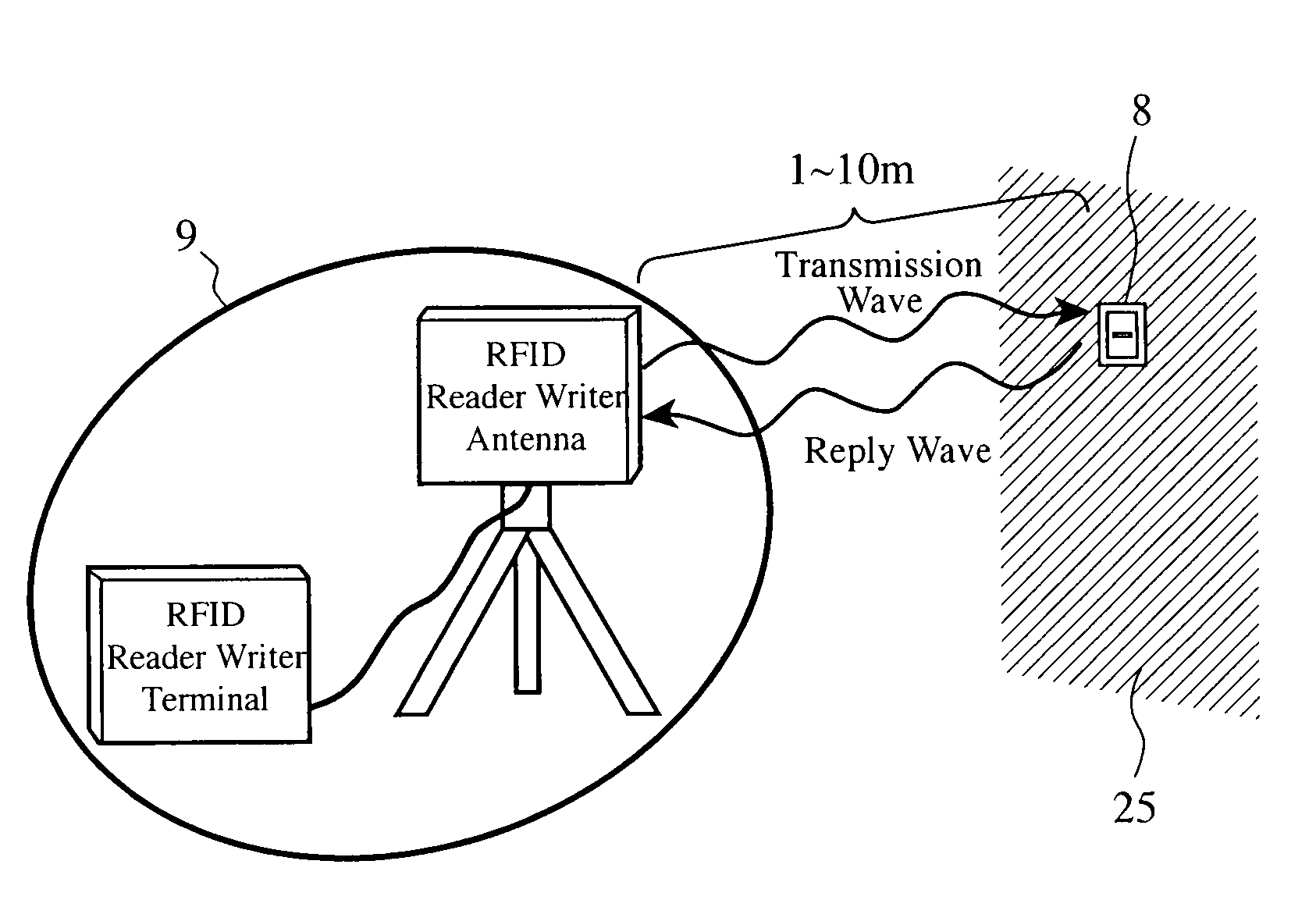
[0132]Embodiment 3 of the present invention will be explained with reference to FIGS. 11 and 12. FIG. 11 shows the structural diagram of an RFID tag in accordance with Embodiment 3, FIG. 11(a) shows a patch conductor surface of the RFID tag, FIG. 11(b) shows a ground conductor surface (with no bonding layer) of the RFID tag, FIG. 11(c) shows a ground conductor surface (with a bonding layer) of the RFID tag, and FIG. 12 is a configuration diagram of an RFID system in accordance with Embodiment 3. In FIGS. 11 and 12, reference numeral 24 denotes a bonding layer, and reference numeral 25 denotes a mounting surface. In the figures, the same reference numerals denote the same components or like components, and the detailed explanation of them will be omitted hereafter. In the RFID tag 8 of FIG. 11, the bonding layer 24 is disposed on a surface of the ground conductor portion 2, and an adhesive bond, a double-faced tape, or the like can be used as the bonding layer 24. A method of applyin...


PUM


Abstract

An RFID tag is characterized in that it includes: a dielectric substrate; a ground conductor portion disposed on one main surface of this dielectric substrate; a patch conductor portion disposed on another main surface of the above-mentioned dielectric substrate and forming a slot; electrical connecting portions internally extending from opposing sides of the above-mentioned slot, respectively; and an IC chip placed in the above-mentioned slot and connected to the above-mentioned electrical connecting portions.

Description

FIELD OF THE INVENTION[0001]The present invention relates to an RFID tag which receives a command signal transmitted from a Radio Frequency Identification (referred to as an RFID from here on) reader writer, which transmits, as a read signal, either information about update or writing of tag information stored in a memory in the RFID tag or the tag information to the RFID reader writer according to information included in the command signal, and which is intended for an RFID system operating in both an UHF band and a microwave band, which is used for entrance / exit control of living bodies and articles, physical distribution management, etc., and a method of manufacturing the RFID tag and a method of mounting the RFID tag.BACKGROUND OF THE INVENTION[0002]An RFID system enables radio communications to be carried out between RFID tags each equipped with an IC chip and an RFID reader writer.RFID tags include active-type tags each of which has a battery therein and runs from the electric...

Claims


Application Information

Patent Timeline
IPC IPC(8): H04Q5/22G08B13/24
CPCG06K19/07749G06K19/07771H01Q1/2225H01Q1/38H01Q13/10G06K19/07G06K19/077H01Q1/24
Inventor OKEGAWA, HIROKATSUMIYAMAE, TAKANORIOHTSUKA, MASATAKANISHIOKA, YASUHIROFUKASAWA, TORUMURAKAMI, OSAMUNAKATANI, TAKASHIKAWANAMI, MASASHI
Owner MITSUBISHI ELECTRIC CORP
Why Eureka
Try Eureka