

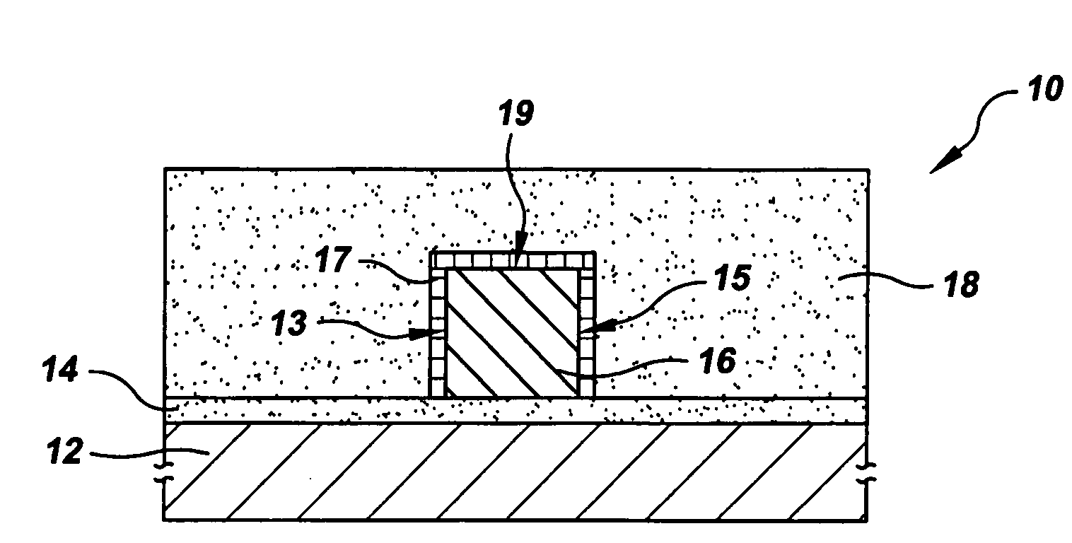
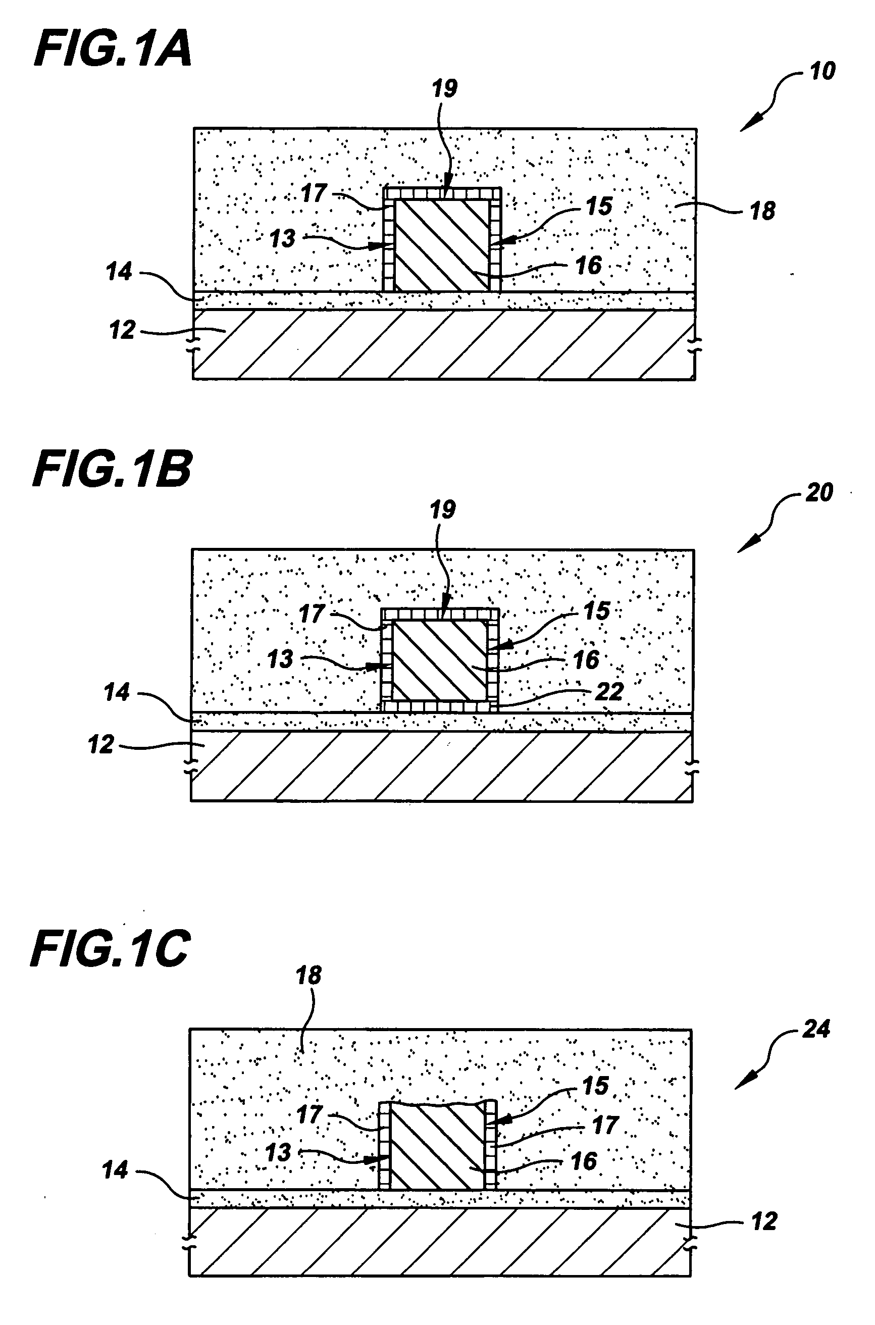
Microphotonic waveguide including core/cladding interface layer
a technology of micro-photonics and waveguides, applied in the field of micro-photonics, can solve the problems of inability to arbitrarily reduce the size of micro-photonic devices, the inability to transport data, and the inability to transmit data, so as to reduce the loss of waveguides
- Summary
- Abstract
- Description
- Claims
- Application Information
AI Technical Summary
Benefits of technology
Problems solved by technology
Method used
Image

Examples
example 1
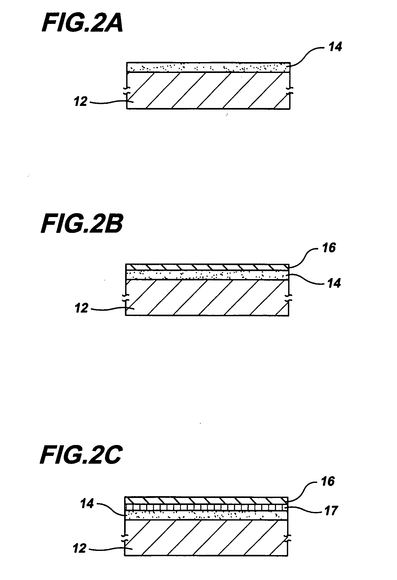
[0127]SOI waveguides were fabricated in the manner described above, with a 200 nm-thick SOI silicon layer and 3 μm-thick buried oxide layer. Deep-UV photolithography was employed to expose the waveguide core mask. Etching of the Si waveguide core was carried out with an Applied Materials DPS poly etch chamber with an HBr / Cl2 / HeO2 / CF4 chemistry. The photoresist was removed with an oxygen plasma ash step. For a number of samples, a 10 nm-thick conformal SiN layer was deposited in the manner described above on the etched Si waveguide core before the top cladding deposition. For all samples, a 3 μm-thick top cladding layer was deposited by high density plasma enhanced chemical vapor deposition from SiH4 and O2 precursors.
[0128]A comparison of average transmission loss data for SOI-based Si / SiO2 waveguides with and without the SiN upper interface layer is plotted in FIG. 7, with the plot showing average waveguide transmission loss for TE polarized light having a wavelength of 1550 nm. Th...
example 2
[0142]Waveguides employing amorphous silicon as a waveguide core material were fabricated in the following manner. A 3 μm-thick HDP-PECVD SiO2 film was deposited on a (100) Si substrate to form an undercladding layer. A thin (10 or 25 nm) PECVD SiN interface layer was subsequently deposited, here to function not only as an interface layer but also to act as an etch stop. Next, a PECVD a-Si waveguide core layer was deposited with one of three deposition powers (P14 precursor was altered and the H-content in the a-Si films was varied. A CMP step was used to remove any top surface roughness that may have been present, leaving a 200 nm-thick a-Si film. Deep TV photolithography at a wavelength, λ=248 nm, and dry etching steps were used to define the single-mode channel waveguides. Post-etch, the resist was removed and another thin, conformal PECVD SiN layer, of 10 nm or 25 nm, was deposited to form an interface layer that operated as a hydrogen diffusion barrier interface layer. Finally,...
PUM
| Property | Measurement | Unit |
|---|---|---|
| thickness | aaaaa | aaaaa |
| thickness | aaaaa | aaaaa |
| refractive index | aaaaa | aaaaa |
Abstract
Description
Claims
Application Information