Method for producing optical coupling element

a coupling element and optical technology, applied in the direction of semiconductor/solid-state device manufacturing, electrical apparatus, semiconductor devices, etc., can solve the problems of lack of versatility, increased labor and time, and easy variation, so as to reduce the number of components and the inventory, suppress the variation of ctr, and determine accurately

Inactive Publication Date: 2008-10-16
SHARP KK
View PDF0 Cites 2 Cited by
  • Summary
  • Abstract
  • Description
  • Claims
  • Application Information

AI Technical Summary

Benefits of technology

[0019]As described above, according to the method for producing an optical coupling element of the present invention, by forming a concave-convex shape in a grid pattern in the front surface of the header portion, the position of each intersection is clearly found from spatial coordinates, the mounting position of each element can be determined accurately, and thus it is possible to mathematically calculate the internal insulation distance. With this, the optimization of CTR can be performed focusing only on the assembly conditions having an internal insulation distance equal to or greater than a predetermined distance, and it is therefore possible to omit unnecessary assembly conditions, and to suppress the variation of CTR. Also, by changing the mounting position of the light-receiving element and the light-emitting element on the front surface of the header portion, the relative position of the light-receiving element and the light-emitting element changes, and the CTR also changes. Accordingly, the need to prepare light-receiving elements of various current amplification factor (hfe) ranks so as to comply with various CTR ranks is eliminated, and thus it is possible to reduce the number of components and the inventory, as well as the variation of output properties.

Problems solved by technology

This production method yields an optical coupling element having a special structure, and thus it cannot be applied to a conventionally used production method in which a light-emitting element and a light-receiving element are mounted on the header portions of a light-emitting side lead frame and a light-receiving side lead frame, respectively, primary molding is performed for these header portions with these elements disposed facing each other, and secondary molding is performed to produce a packaged optical coupling element.
For this reason, the above method has the problem of lack of versatility.
However, the method of Conventional Technology 1 described above has the problem that even if a light-receiving element and a light-emitting element are mounted in the marked positions with good accuracy, when the CTR of the produced optical coupling element is different from the desired CTR, it is necessary to provide an additional mark at another position of the front surface of the header portion of the lead frames by processing, in order to remount the elements in a different location, which requires additional labor and time.
Particularly, response property, which is one of the important properties of optical coupling elements, is easily affected by current amplification factors (hfe), and thus there has been the problem that a variation easily occurs in the response property of an optical coupling element obtained by introducing different current amplification factor (hfe) ranks.

Method used


Image

  • Method for producing optical coupling element
  • Method for producing optical coupling element
  • Method for producing optical coupling element

Examples


Embodiment Construction

[0024]Hereinafter, an embodiment of the present invention will be described with reference to the accompanying drawings.

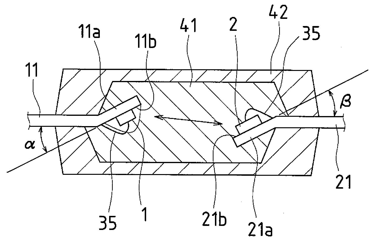
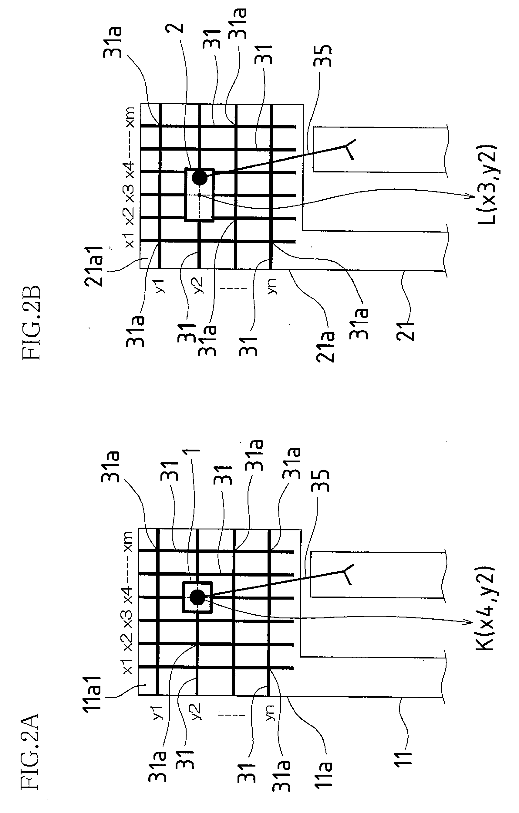
[0025]FIG. 1 is a cross-sectional view that shows the structure of an optical coupling element obtained by applying a production method of the present invention. FIG. 2A is a plan view that shows a light-emitting element mounted on the front surface of the header portion of a lead frame for a light-emitting element, and FIG. 2B is a plan view that shows a light-receiving element mounted on the front surface of the header portion of a lead frame for a light-receiving element.

[0026]The optical coupling element of the present embodiment has a structure formed as follows. A light-emitting element 1 is mounted onto a front surface 11b of a header portion 11a of a light-emitting side lead frame 11, and a light-receiving element 2 is mounted onto a front surface 21b of a header portion 21a of a light-receiving side lead frame 21. After that, the light-emitting element 1 a...


PUM


Abstract

A method for producing an optical coupling element of the present invention includes the steps of: determining the mounting position of a light-emitting element and a light-receiving element on the front surface of the header portion of each lead frame based on the current amplification factor of the light-receiving element to be mounted; determining the bending angle of each header portion and a distance between the two elements after being bent by calculation such that a predetermined current transfer ratio and an internal insulation distance required by the optical coupling element to be produced are obtained; detecting the determined mounting position by detecting intersections of V-shaped grooves in a grid pattern formed on the front surface of each header portion; mounting each element onto the detected position of the front surface of each header portion while detecting the concave-convex shape; and bending each header portion after mounting each element at the bending angle determined by calculation.

Description

BACKGROUND OF THE INVENTION[0001]This application claims priority under 35 U.S.C. §119(a) on Patent Application No. 2007-104189 filed in Japan on Apr. 11, 2007, the entire contents of which are hereby incorporated herein.[0002]The present invention relates to a method for producing an optical coupling element that transmits signals by a light-emitting element and a light-receiving element, and more particularly to a method for producing an optical coupling element that can secure a predetermined internal insulation distance.[0003]Generally, the current transfer ratio, which is the ratio of input forward current and output current, is a main property of optical coupling elements. This CTR value is required to fall within a predetermined range wherever possible in designing a circuit in which the optical coupling element is incorporated.[0004]Also, the internal insulation distance is an important indicator to determine the insulation property of an insulation type optical coupling ele...

Claims


Application Information

Patent Timeline
Patent Type & Authority Applications(United States)
IPC IPC(8): H01L33/00H01L31/18H01L31/12
CPCH01L31/167
Inventor KITAMURA, TAKESHI
Owner SHARP KK
Why Eureka
Try Eureka