Terminal for engaging type connector
- Summary
- Abstract
- Description
- Claims
- Application Information
AI Technical Summary
Benefits of technology
Problems solved by technology
Method used
Image

Examples
first embodiment
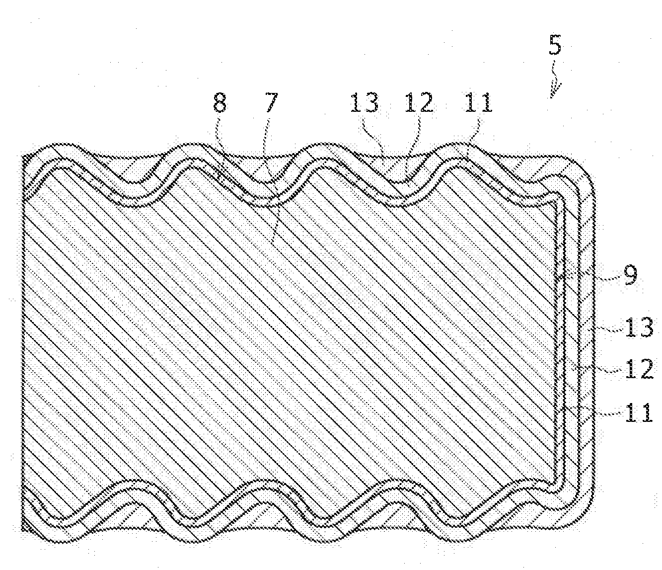
[0051]A terminal in a first embodiment according to the present invention for an engaging type connector and a method of manufacturing the same will be described with reference to FIGS. 1 to 6.
[0052]The terminal, which is assumed to be a pin terminal for a printed wiring board, is manufactured by the following steps.
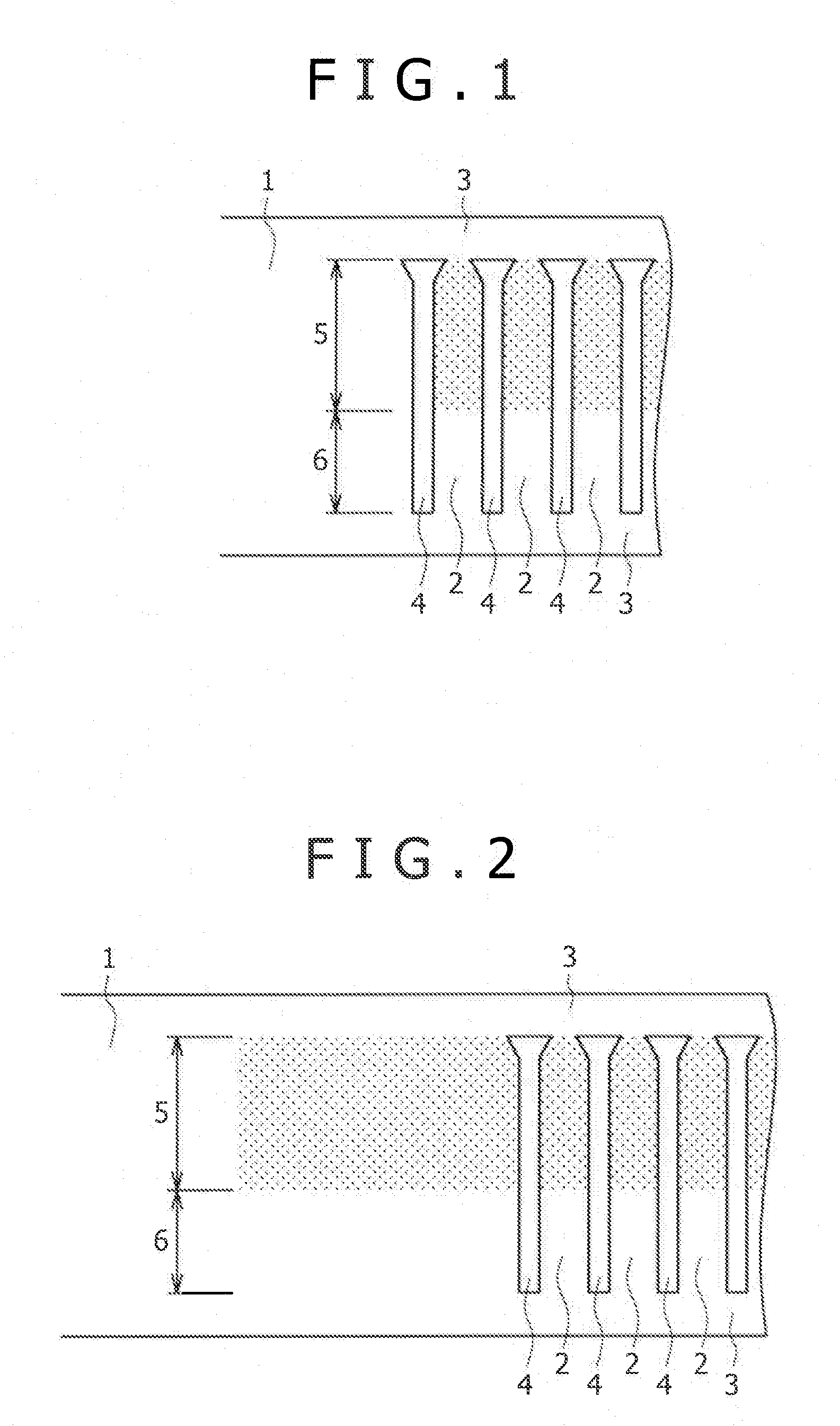
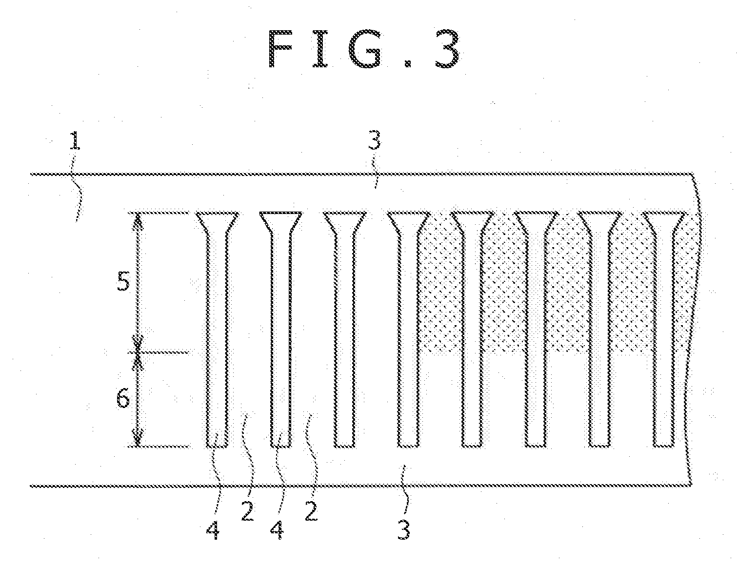
[0053](1) Referring to FIG. 1, a normally rolled Cu alloy strip 1 is subjected to a punching process by a progressive die to form longitudinally arranged terminal bodies 2 connected by connecting parts 3. Indicated at 4 are openings formed by the punching process.
[0054]The surfaces of engaging parts 5 of the terminal bodies 2 are roughened by press work concurrently with the punching process. In FIG. 1, parts shaded by small dots are engaging parts 5 having the rough surfaces. The surface roughness of solder-bonding parts 6 of the terminal bodies 2 are the same as the original surface roughness of the Cu alloy strip 1. The press work is executed before the Cu strip 1 is ...
second embodiment
[0075]A terminal in a second embodiment according to the present invention for an engaging type connector and a method of manufacturing the same will be described with reference to FIGS. 11 to 13, in which parts like or corresponding to those of the first embodiment are designated by the same reference characters.
[0076]The terminal, which is assumed to be a pin terminal for a printed wiring board, is manufactured by the following steps.
[0077](1) Referring to FIG. 11A, a Cu alloy strip 1 is subjected to a punching process to form longitudinally arranged terminal bodies 2 connected by connecting parts 3. The surface of the Cu alloy strip 1 has an arithmetic mean roughness Ra of 0.15 μm or above at least with respect to one direction and an arithmetic mean roughness Ra of 4.0 μm or below with respect to all directions. Indicated at 4 are openings formed by the punching process. FIG. 11A shows the Cu alloy strip 1 in a state after a postplating process.
[0078](2) The entire surface of th...
example 1
[0127]Example 1 of the present invention will be shown.
[0128]Preparation of Test Samples
[0129]Processes used for making test samples Nos. 1 to 31 are shown in Tables 1 and 2.
[0130]A Cu alloy plate containing Cu, 1.8% by mass Ni, 0.40% by mass Si, 0.10% by mass Sn and 1.1% by mass Zn was processed to provide base materials. The surface of the Cu alloy plate was roughened by using a work roll having a surface roughened by shot blasting for rolling (or not roughened) to provide base materials having a Vickers hardness 200, a thickness of 0.25 mm, and different surface roughnesses, respectively. The respective surface roughnesses of parts of the base materials corresponding to engaging parts of test samples are shown in Tables 3 and 4. The respective surface roughnesses Ra of parts of the base materials corresponding to solder-bonding parts of all the test samples Nos. 1 to 31 are 0.05 μm.
[0131]A plated Ni layer (or no plated Ni layer), a plated Cu layer (or no plated Cu layer) and a pl...
PUM
| Property | Measurement | Unit |
|---|---|---|
| Length | aaaaa | aaaaa |
| Length | aaaaa | aaaaa |
| Length | aaaaa | aaaaa |
Abstract
Description
Claims
Application Information
 - Generate Ideas
- Intellectual Property
- Life Sciences
- Materials
- Tech Scout
- Unparalleled Data Quality
- Higher Quality Content
- 60% Fewer Hallucinations
Browse by: Latest US Patents, China's latest patents, Technical Efficacy Thesaurus, Application Domain, Technology Topic, Popular Technical Reports.
© 2025 PatSnap. All rights reserved.Legal|Privacy policy|Modern Slavery Act Transparency Statement|Sitemap|About US| Contact US: help@patsnap.com