Light Emitting Diode

Inactive Publication Date: 2008-10-23
SEOUL OPTO DEVICE CO LTD
View PDF5 Cites 9 Cited by
  • Summary
  • Abstract
  • Description
  • Claims
  • Application Information

AI Technical Summary

Benefits of technology

[0025]As described above, in the present invention, an active layer having a quantum well structure is formed using AlGaN well layers and AlN barrier layers such that the characteristics of the active layer can be improved. Therefore, far-ultraviolet light with an emission wavelength of 200 nm to 300 nm can be easily emitted and the optical power of a light emi

Problems solved by technology

However, according to the InxGa1-xN, it is difficult to emit

Method used


Image

  • Light Emitting Diode
  • Light Emitting Diode
  • Light Emitting Diode

Examples


Embodiment Construction

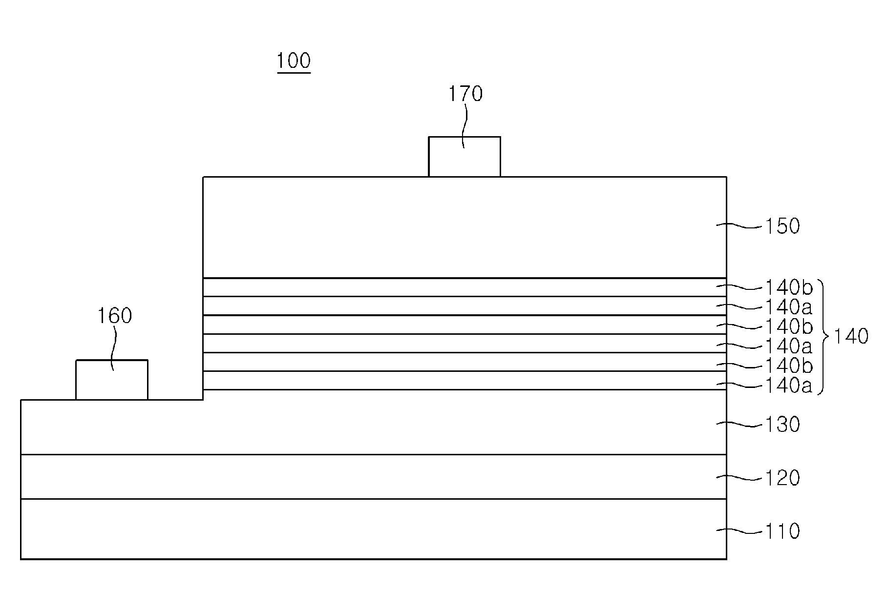
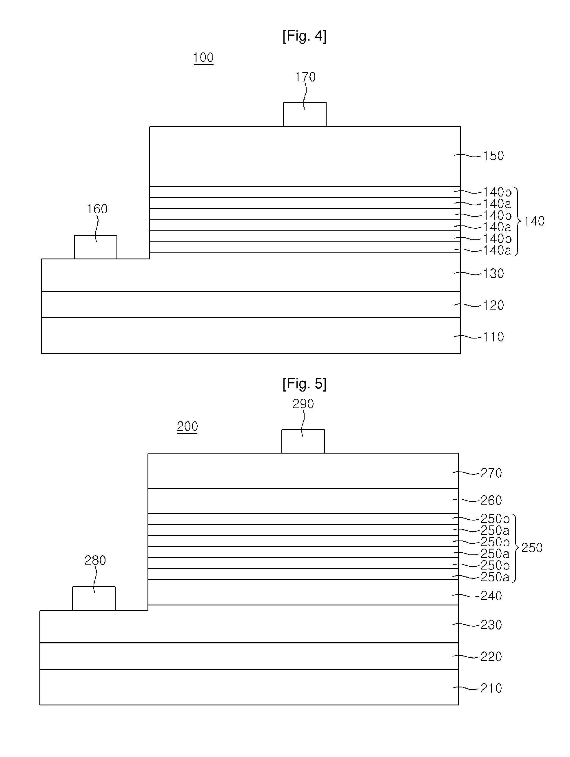
[0032]Hereinafter, preferred embodiments of the present invention will be described in detail with reference to the accompanying drawings.

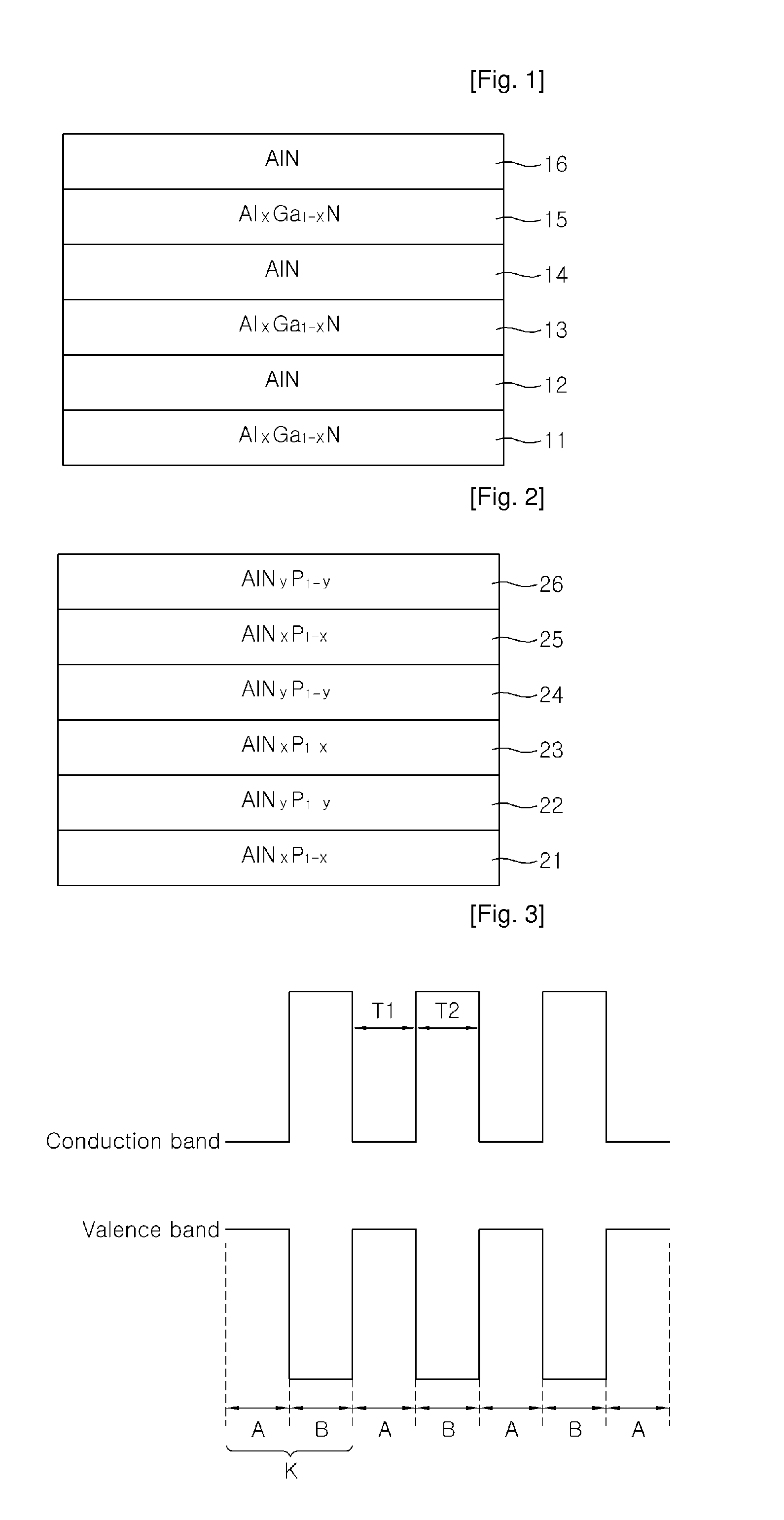
[0033]FIG. 1 is a sectional view illustrating an active layer having a quantum well structure according to an embodiment of the present invention, and FIG. 3 is an energy diagram of an active layer.

[0034]Referring to FIG. 1, an active layer according to an embodiment of the present invention comprises AlxGa1-xN (0≦x≦1) well layers 11, 13 and 15 and AlN barrier layers 12, 14 and 16, wherein a plurality of well layers and a plurality of barrier layers are alternately laminated at least once. In such a quantum well structure, a barrier layer B has high conduction band energy and low valence band energy whereas a well layer A has low conduction band energy and high valence band energy, as illustrated in an energy diagram of FIG. 3. Therefore, the barrier layer B has an energy band gap greater than the well layer A.

[0035]In order to form an active laye...


PUM


Abstract

The present invention relates to a light emitting diode. More specifically, the present invention relates to a light emitting diode comprising an N-type semiconductor layer formed on a substrate, an active layer formed on the N-type semiconductor layer and a P-type semiconductor layer formed on the active layer, wherein the active layer is formed to have either a quantum well structure in which an AlxGa1-xN (0≦x<1) well layer and an AlN barrier layer are alternately laminated or a quantum well structure in which a well layer and a barrier layer are formed of a compound semiconductor layer containing phosphorous (P) and are alternately laminated. Accordingly, far-ultraviolet light can be easily emitted and the optical power of the light emitting diode can also be improved.

Description

TECHNICAL FIELD[0001]The present invention relates to a compound semiconductor light emitting diode, and more particularly, to a compound semiconductor light emitting diode which comprises either an active layer having a quantum well structure consisting of an AlxGa1-xN well layer and an AlN barrier layer or an active layer having a quantum well structure consisting of an AlNP well layer and an AlNP barrier layer such that far-ultraviolet light can be easily emitted and the optical power thereof can be improved.BACKGROUND ART[0002]A light emitting diode is basically a semiconductor PN junction diode. When joining P-type and N-type semiconductors with each other and then applying voltage to the joined P-type and N-type semiconductors, holes of the P-type semiconductor move toward the N-type semiconductor and gather in a middle layer whereas electrons of the N-type semiconductor move toward the P-type semiconductor and gather in a middle layer that is a lowermost portion of a conducti...

Claims


Application Information

Patent Timeline
IPC IPC(8): H01L33/00H01L33/06H01L33/12H01L33/32
CPCB82Y20/00H01L33/06H01L33/32
Inventor KIM, KYOUNG HOON
Owner SEOUL OPTO DEVICE CO LTD
Why Eureka
Try Eureka