Process for realizing an integrated electronic circuit with two active layer portions having different crystal orientations

a technology of active layer and crystal orientation, which is applied in the direction of basic electric elements, solid-state devices, electric apparatus, etc., can solve the problems of high design and fabrication cost, particularly high cost of dual-soi substrate, and achieve the effect of reducing the electrical resistance in the on-sta

Active Publication Date: 2008-10-23
STMICROELECTRONICS (CROLLES 2) SAS
View PDF14 Cites 9 Cited by
  • Summary
  • Abstract
  • Description
  • Claims
  • Application Information

AI Technical Summary

Benefits of technology

[0013]One object of the invention is therefore to realize in an economic manner an electronic circuit chip which comprises both n-type an...

Problems solved by technology

The integrated electronic circuit which is obtained is therefore a hybrid, making its design and fabrication ...

Method used


Image

  • Process for realizing an integrated electronic circuit with two active layer portions having different crystal orientations
  • Process for realizing an integrated electronic circuit with two active layer portions having different crystal orientations
  • Process for realizing an integrated electronic circuit with two active layer portions having different crystal orientations

Examples


Embodiment Construction

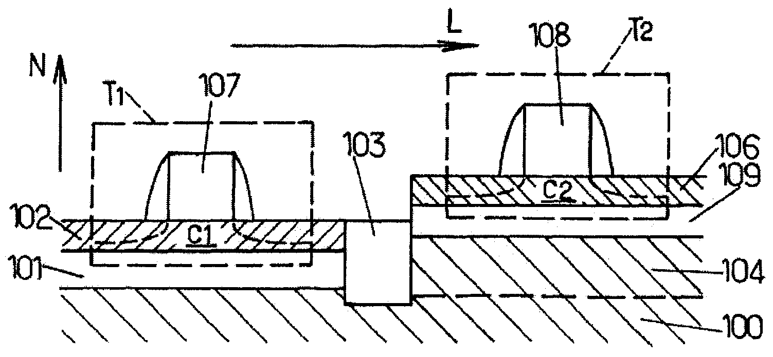
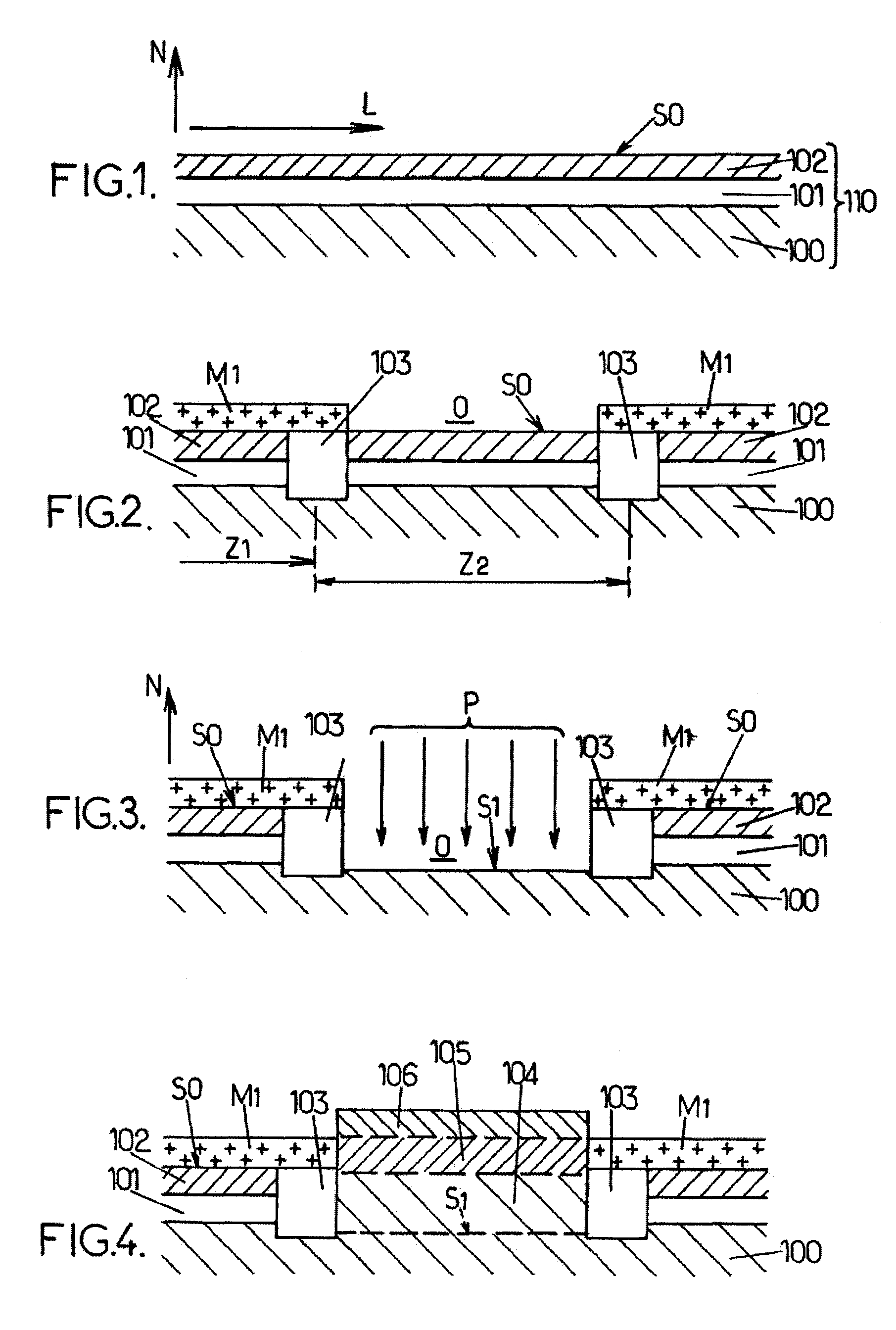
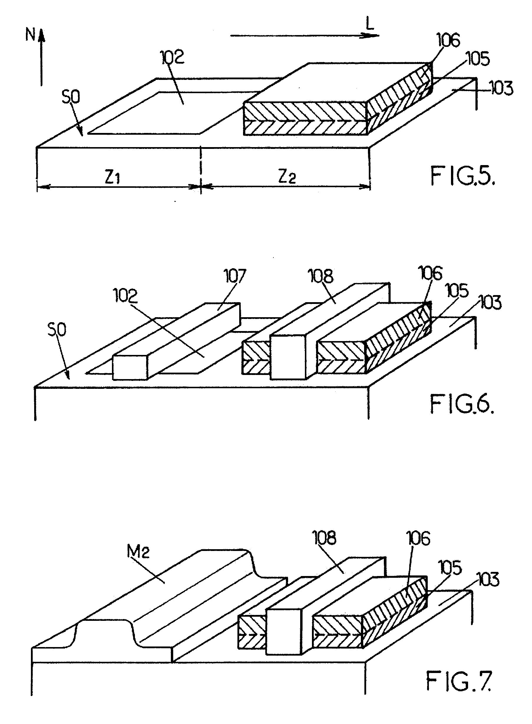
[0044]For clarity, the sizes of the various elements represented in these figures do not correspond to the actual sizes or size ratios. In addition, the same references appearing in different figures indicate the same elements. FIGS. 1-4 and 11 are sectional views of an integrated electronic circuit during its fabrication, and FIGS. 5-10 are perspective views of the same circuit at different steps in the process. The substrate of the circuit is found in the lower part of all figures, and N indicates a direction perpendicular to a flat surface S0 of the substrate, pointing towards the top of the figures. The words “on”, “under”, “above”, and “below” used below are in reference to this orientation.

[0045]Now a process will be described for realizing the circuit of the invention, citing the steps for doing so in one possible order. Each of the steps is not described in detail regarding its implementation parameters, as such information is known to a person skilled in the art.

[0046]As sh...


PUM


Abstract

A process for realizing an integrated electronic circuit makes it possible to obtain transistors with p-type conduction and transistors with n-type conduction, in respective active zones having crystal orientations adapted to each conduction type. In addition, each active zone is electrically insulated from a primary substrate of the circuit, so that the entire circuit is compatible with SOI technology.

Description

BACKGROUND[0001]1. Technical Field[0002]This invention relates to a process for realizing an integrated electronic circuit comprising two active layer portions with different crystal orientations. Such a circuit can be CMOS, or “Complementary Metal-Oxide-Semiconductor” in the terminology of a person skilled in the art. It also relates to an integrated electronic circuit of the type obtained by such a process.[0003]2. Description of the Related Art[0004]CMOS integrated electronic circuits contain MOS transistors with n-type conduction (nMOS) and MOS transistors with p-type conduction (pMOS).[0005]The channel of a MOS transistor commonly has a monocrystalline portion based on silicon, to reduce the electrical resistance of the transistor in the on state. “Monocrystalline portion” is understood to mean a portion of crystalline material in which the crystal orientation does not substantially vary across this portion, in spite of the presence of any defects. Such defects may be dislocati...

Claims


Application Information

Patent Timeline
IPC IPC(8): H01L29/00H01L21/76
CPCH01L21/823807H01L21/823828H01L21/823878H01L21/84
Inventor BOEUF, FREDERIC
Owner STMICROELECTRONICS (CROLLES 2) SAS
Why Eureka
Try Eureka