Surface-roughening method

a surface roughening and surface technology, applied in semiconductor/solid-state device manufacturing, electrical equipment, semiconductor devices, etc., can solve the problem of unerringly creating surface unevenness in the order of tens or hundreds of nanometers, affecting the efficiency of led machining, and difficult to achieve the effect of smoothing desired work surfaces more easily and inexpensively

Active Publication Date: 2008-10-23
SANKEN ELECTRIC CO LTD
View PDF5 Cites 25 Cited by
  • Summary
  • Abstract
  • Description
  • Claims
  • Application Information

AI Technical Summary

Benefits of technology

[0007]The present invention has it as an object to roughen desi

Problems solved by technology

Those of the light rays radiated in various directions in the semiconductor chip which impinge on the boundary surface at angles greater than the critical angle with respect to the normal to the surface are totally reflected away therefrom, with a consequent drop in the efficiency of the LED.
Blade mac

Method used


Image

  • Surface-roughening method
  • Surface-roughening method
  • Surface-roughening method

Examples


Embodiment Construction

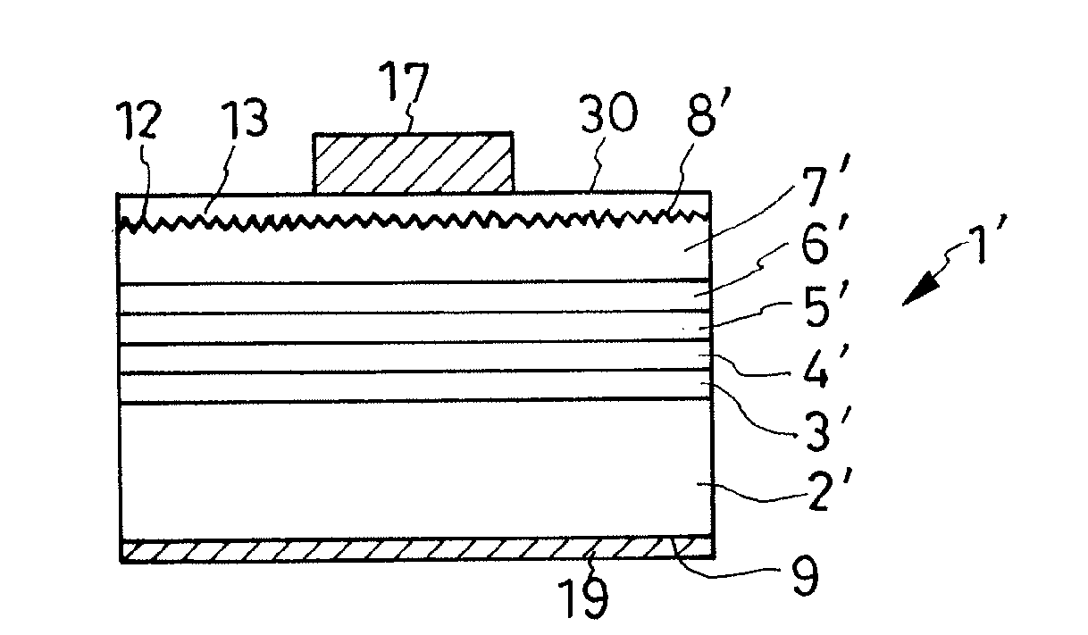
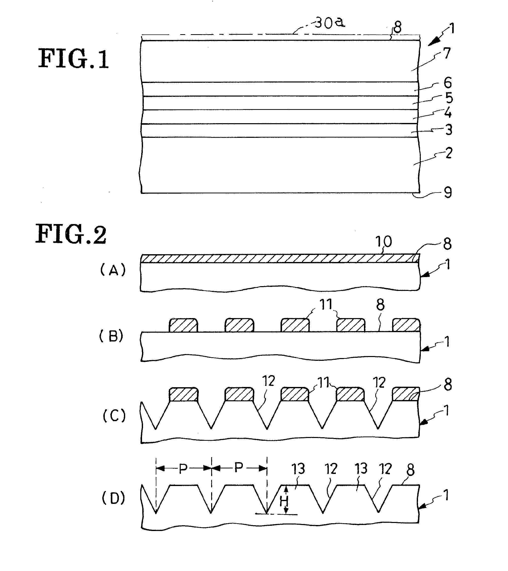
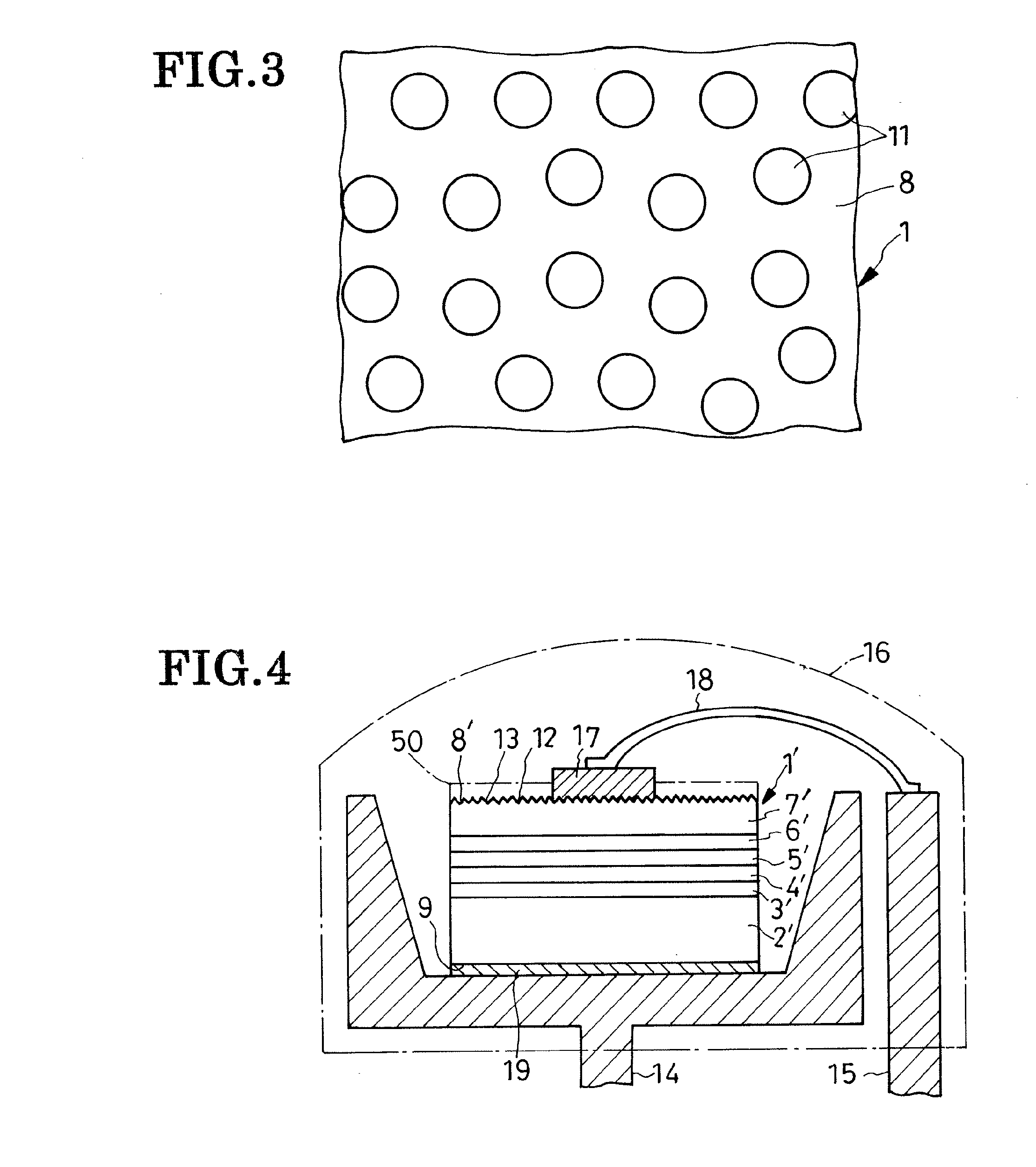
[0022]The particulate mask surface-roughening method according to the present invention will now be described more specifically as applied by way of example to an LED wafer of known double heterojunction design, which is to be subsequently diced into LED chips or dies. As pictured in FIG. 1, the exemplified double heterojunction LED wafer I has a substrate 2 on which there are successively grown a buffer 3, an n-type semiconductor layer or lower cladding 4, an active layer 5, a p-type semiconductor layer or upper cladding 6, and a supplementary layer 7.

[0023]The substrate 2 is of silicon doped with either n- or p-type impurity to possess electric conductivity. Alternatively, the substrate 2 may be made from any such known or suitable materials as sapphire, ceramics, or semiconductors other than silicon.

[0024]The buffer 3 is multilayered, having multiple alternations of an aluminum nitride and a gallium nitride layer grown by epitaxy. A monolayered buffer is adoptable instead. It is ...


PUM


Abstract

The method is disclosed as applied to roughening the light-emitting surface of an LED wafer for reduction of the internal total reflection of the light generated. A masking film of silver is first deposited on the surface of a wafer to be diced into LED chips. Then the masking film is heated to cause its coagulation into discrete particles. Then, using the silver particles as a mask, the wafer surface is dry etched to create pits therein. The deposition of silver on the wafer surface and its thermal coagulation into particles may be either successive or concurrent.

Description

CROSS REFERENCE TO RELATED APPLICATIONS[0001]This application claims priority to Japanese Patent Application No. 2007-109272, filed Apr. 18, 2007.BACKGROUND OF THE INVENTION[0002]This invention relates to a method of roughening solid surfaces, that is, creating a multiplicity of closely spaced pits and projections on or in such surfaces. The invention lends itself to the surface roughening of light-emitting semiconductor devices, or light-emitting diodes (LEDs) in more common parlance, for reduction of internal total reflection of the light, and of semiconductor substrates for epitaxial growth of low-dislocation-density layers thereon, among other applications.[0003]An LED may be envisaged for the purposes of the invention as a combination of a light-generating chip of semiconducting material and a protective envelope of transparent plastic material therefor. The semiconductor chip of familiar design has a set of layers for generating light, and a supplementary layer (termed various...

Claims


Application Information

Patent Timeline
IPC IPC(8): H01L33/00H01L21/302H01L33/06H01L33/22H01L33/32H01L33/56
CPCH01L33/22H01L2224/48091H01L2224/48247H01L2224/73265H01L2224/48472H01L2224/32245H01L2924/00014H01L2924/00H01L2924/00012
Inventor MATSUO, TETSUJITAZIMA, MIKIOKATO, TAKASHI
Owner SANKEN ELECTRIC CO LTD
Why Eureka
Try Eureka