Semiconductor device and method of forming gate and metal line thereof

a semiconductor device and metal line technology, applied in the field of semiconductor devices, can solve the problems of difficult operation of optical proximity correction, change in electrical characteristics of transistors, and difficulty in ensuring the stability of metal line patterns

Inactive Publication Date: 2008-10-30
SK HYNIX INC
View PDF13 Cites 17 Cited by
  • Summary
  • Abstract
  • Description
  • Claims
  • Application Information

AI Technical Summary

Benefits of technology

[0034]It is an objective of the present invention to provide a pattern that is capable of ensuring e

Problems solved by technology

Such a variation in the line width of the gate may cause changes in the electrical characteristics of the transistor, and a problem is caused in that it is difficult to operate an optical proximity correction for ensuring a uniform variation in the line width.
Therefore, a problem exists,

Method used


Image

  • Semiconductor device and method of forming gate and metal line thereof
  • Semiconductor device and method of forming gate and metal line thereof
  • Semiconductor device and method of forming gate and metal line thereof

Examples


Embodiment Construction

[0092]Hereinafter, preferred embodiments of the present invention will be described in detail with reference to the accompanying drawings.

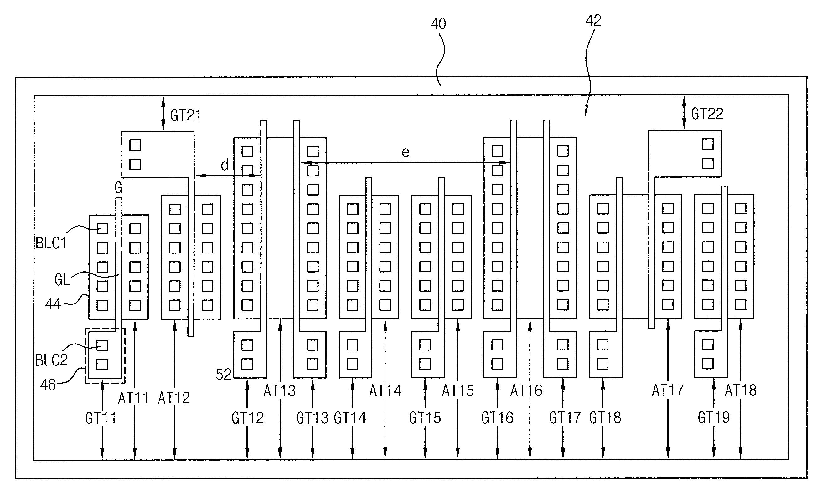
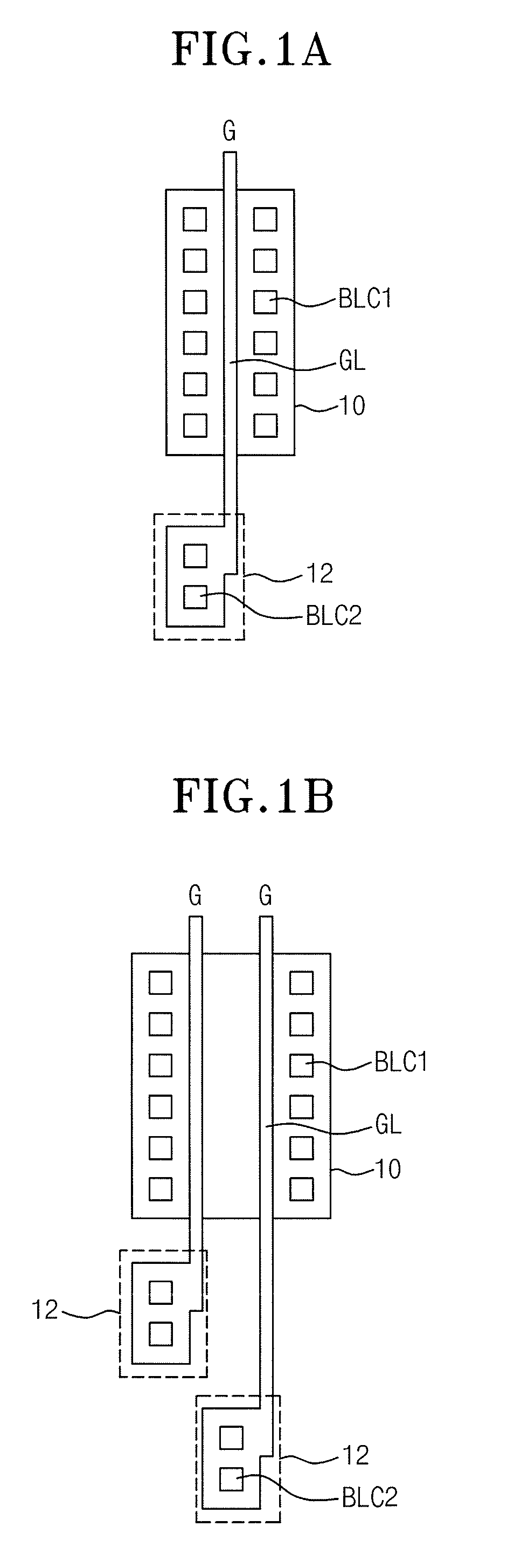
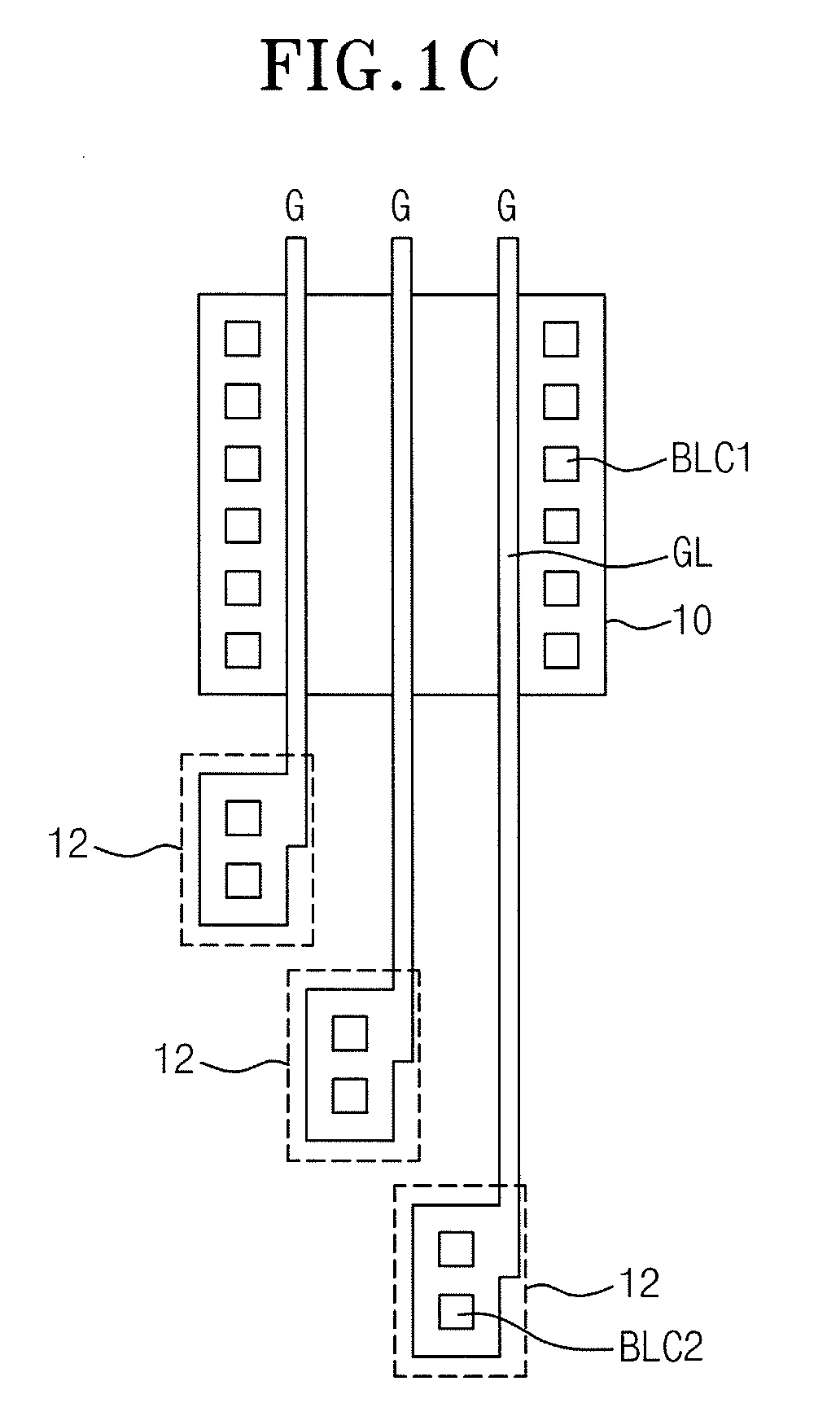
[0093]A semiconductor device of the present invention includes a plurality of MOS transistors aligned in a line formation within a predetermined well region. A gate of the MOS transistor includes an integrated gate line and a gate pad, and the gate pad is disposed on the same surface as the gate line with respect to an extended line of an edge of the gate line and aligned so that a side thereof adjoins the extended line.

[0094]More specifically, the semiconductor device of the present invention includes a predetermined MOS transistor, and the gate of the MOS transistor has a structure wherein a gate line, which is formed over an active region of the MOS transistor, and a gate pad, which is electrically connected to a metal line of an upper layer of the MOS transistor, are integrated. Herein, the gate may have shapes as shown in FIGS. 8A through 8E....


PUM


Abstract

A gate in a semiconductor device is formed to have a dummy gate pattern that protects a gate. Metal lines are formed to supply power for a semiconductor device and transfer a signal. A semiconductor device includes a quad coupled receiver type input/output buffer. The semiconductor device is formed with a gate line that extends over an active region, and a gate pad located outside of the active region. The gate line and the gate pad are adjoined such that the gate line and a side of the gate pad form a line. Dummy gates may also be applied. The semiconductor device includes a first metal line patterns supplying power to a block having a plurality of cells, a second metal line pattern transferring a signal to the cells, and dummy metal line patterns divided into in a longitudinal direction.

Description

CROSS-REFERENCE TO RELATED APPLICATIONS[0001]The present application claims priority to Korean patent application numbers 10-2007-0042250, 10-2007-0046255, 10-2007-0047021, 10-2007-0048628, 10-2007-0065485 filed or, Apr. 30, 2007, May 11, 2007, May 15, 2007, May 18, 2007, Jun. 29, 2007, respectively, which are incorporated herein by reference in their entirety.BACKGROUND OF THE INVENTION[0002]The present invention relates generally to a semiconductor device, and more particularly to a method of forming a gate of a semiconductor device, the gate having a dummy gate pattern that protects a gate pattern, a method of forming a metal line that supplies the power for a semiconductor device and transfers a signal, and a semiconductor device including a quad coupled receiver type input / output buffer.[0003]In general, a typical semiconductor device includes devices such as transistors, capacitors, and resistors, and is formed with wirings that electrically connect the devices to one another....

Claims


Application Information

Patent Timeline
IPC IPC(8): H01L27/088H01L21/28
CPCH01L27/0207Y10S438/926
Inventor RYU, NAM GYUKIM, HO RYONGCHOI, WON JOHNKIM, JAE HWANKANG, SEOUNG HYUNYOON, YOUNG HEE
Owner SK HYNIX INC
Why Eureka
Try Eureka