

Liquid epoxy resin composition and semiconductor device
a technology of epoxy resin and semiconductors, applied in semiconductor devices, solid-state devices, basic electric elements, etc., can solve the problems of reducing affecting the reliability of semiconductor packages, and low productivity of the process, so as to improve the working efficiency, reduce the cost of manufacturing, and improve the reliability of semiconductor devices. , the effect of high productivity
Inactive Publication Date: 2008-10-30
SHIN ETSU CHEM IND CO LTD
View PDF9 Cites 36 Cited by
- Summary
- Abstract
- Description
- Claims
- Application Information
AI Technical Summary
Benefits of technology
[0009]The inventor has found that incorporation of a hygroscopic agent in an epoxy resin composition for use as no-flow underfill results in an epoxy resin composition for semiconductor encapsulation meeting a commercially viable combination of void-free fill, solder connection, and reliability.
[0017]The liquid epoxy resin composition for use as no-flow underfill according to the invention is improved in working efficiency, void-free fill, solder connection, and adhesion, and thus advantageously used in the fabrication of flip chip semiconductor devices by the no-flow method featuring a high productivity. This ensures that highly reliable semiconductor devices are fabricated.
Problems solved by technology
Thus the process suffers from a low productivity.
Additionally, the flux removal by cleaning becomes inefficient as the width of and the pitch between solder electrodes are reduced.
The flux residue can interfere with wetting of the sealing resin, and ionic impurities in the flux residue detract from the reliability of semiconductor packages.
Many technical problems remain unsolved in association with the flux.
However, since the heating operation for pressure bonding between the substrate and the semiconductor chip and curing the resin is conducted within a brief time, and since bonding of lead-free solder materials is conducted at higher temperatures than in the prior art, the problem of voids generated in the encapsulating resin becomes significant.
Method used
View moreImage
Smart ImageViewing Examples

Examples
example
[0054]Examples of the invention are given below by way of illustration and not by way of limitation. Unless otherwise stated, all percents and parts are by weight.
Login to View More PUM
| Property | Measurement | Unit |
|---|---|---|
| Specific surface area | aaaaa | aaaaa |
Abstract
A liquid epoxy resin composition comprising (A) a liquid epoxy resin, (B) a curing agent, (C) an inorganic filler, (D) a hygroscopic agent, and optionally, (E) a fluxing agent has the advantages of void-free fill, shelf stability and solder connection, and is thus advantageously used in the fabrication of flip chip semiconductor devices by the no-flow method.
Description
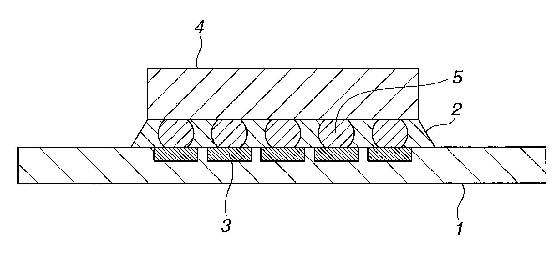
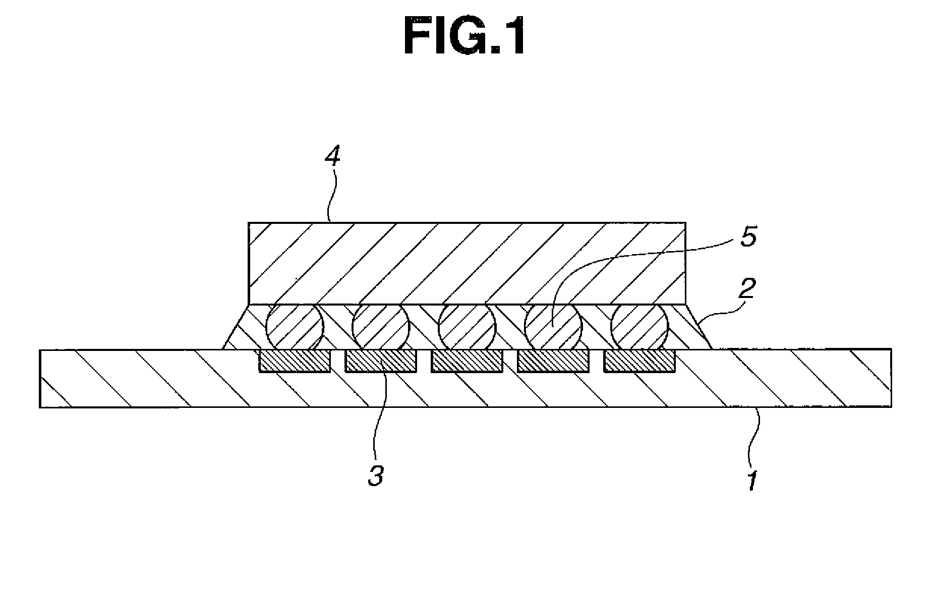
CROSS-REFERENCE TO RELATED APPLICATION[0001]This non-provisional application claims priority under 35 U.S.C. §119(a) on Patent Application No. 2007-118607 filed in Japan on Apr. 27, 2007, the entire contents of which are hereby incorporated by reference.TECHNICAL FIELD[0002]This invention relates to liquid epoxy resin compositions for use as no-flow underfill which are void-free, reliable and effectively workable, and facilitate the process of fabricating semiconductor devices, especially flip chip semiconductor devices, and flip chip semiconductor devices encapsulated with the epoxy resin compositions.BACKGROUND ART[0003]To meet the modern demand for further reducing the size, profile and weight of semiconductor packages, a significant increase in the density of semiconductor chips has been achieved. A typical technique of mounting high density semiconductor chips is flip-chip mounting which is on wide-spread use. A typical flip-chip mounting technique is the controlled collapse ch...
Claims
Login to View More Application Information
Patent Timeline
 IPC IPC(8): H01L23/16C08L63/00C08K3/36
CPCC08G59/4215C08G59/5033C08G59/621C08K3/36C08K5/175C08L63/00H01L21/563H01L23/295H01L23/296H01L23/3121H01L2224/73203H01L2924/01012H01L2924/0102H01L2924/01077H01L2924/12044H01L2924/01019H01L2224/16225H01L2224/32225H01L2224/73204H01L2924/00H01L2924/00011H01L2924/00014H01L2224/0401H01L2924/00012
InventorASANO, MASATOSHI
OwnerSHIN ETSU CHEM IND CO LTD