Semiconductor Device Testing Apparatus and Power Supply Unit

a technology of electromagnetic field and test apparatus, applied in the field of testing apparatus, can solve the problem of not being able to achieve the desired contact force by itself, and achieve the effect of reducing costs, narrowing pitch, and high reliability of connections

Inactive Publication Date: 2008-10-30
NEC CORP
View PDF6 Cites 59 Cited by
  • Summary
  • Abstract
  • Description
  • Claims
  • Application Information

AI Technical Summary

Benefits of technology

[0090]In accordance with the present invention, contact marks on the electrodes of a semiconductor device, i.e., a tested LSI, can be prevented from forming, whereby highly reliable connections can be formed in the subsequent connection process, and a device having a narrower pitch and dramatically lower costs can be made possible. Testing can be carried out at a higher speed than in conventional testing by using a testing LSI, and selective testing at the same level as a packaged product can be performed with the semiconductor device in a bare chip state. Therefore, the production yield rate for a SiP (System in Package) in which a bare chip is used can be increased and manufacturing costs can be considerably reduced.

Problems solved by technology

The flexible substrate 170 is thin and therefore cannot achieve a desired contact force by itself.

Method used


Image

  • Semiconductor Device Testing Apparatus and Power Supply Unit
  • Semiconductor Device Testing Apparatus and Power Supply Unit
  • Semiconductor Device Testing Apparatus and Power Supply Unit

Examples


first embodiment

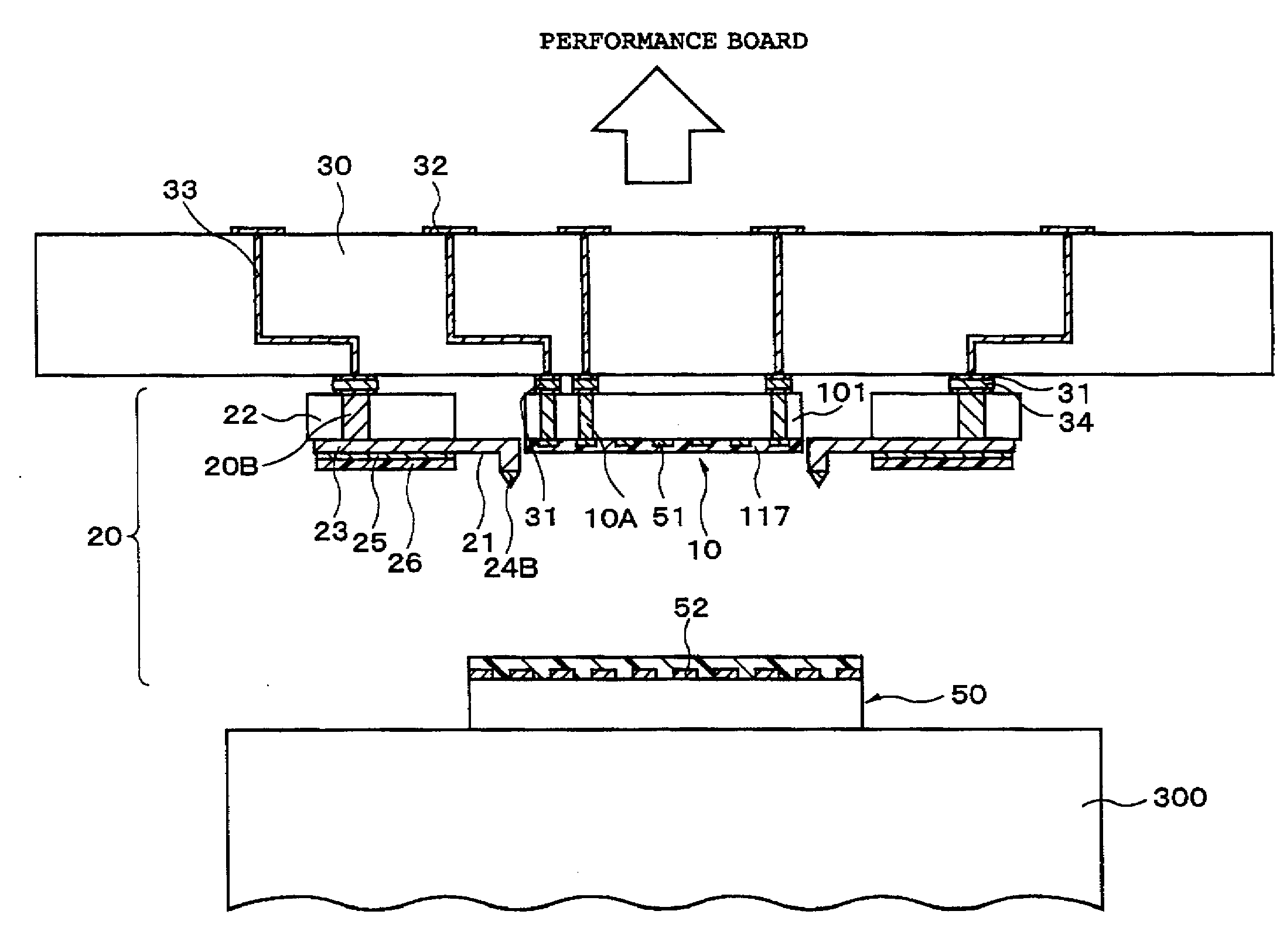
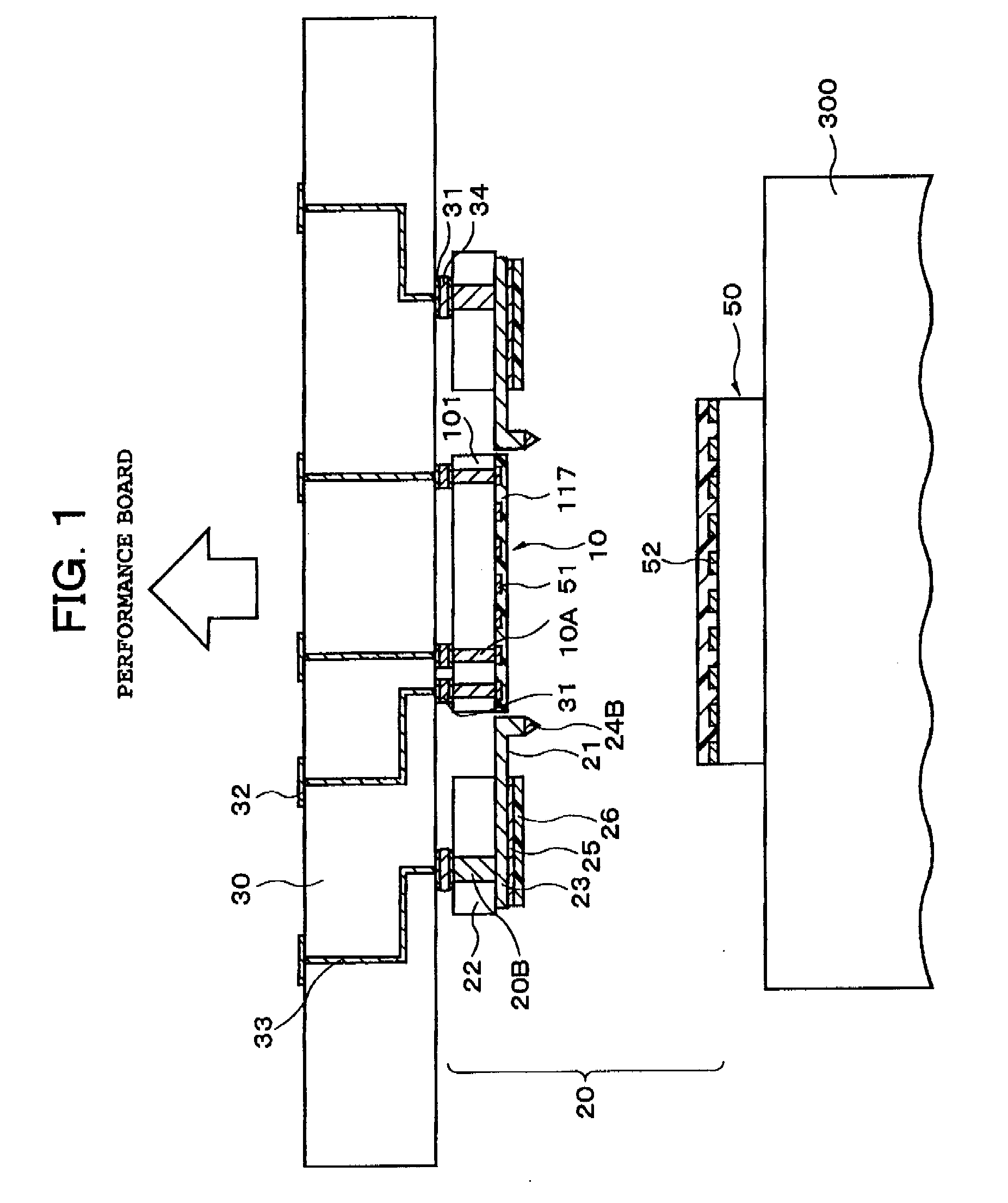
[0131]FIG. 1 is a cross-sectional view showing the semiconductor device testing apparatus according to a first embodiment of the present invention, and more particularly shows the details of the power supply unit and the probe section of the power supply unit. The entire configuration of the present embodiment will be described first. The semiconductor device testing apparatus according to the present embodiment is composed of a testing LSI 10, a power supply unit 20, and an intermediate substrate 30, as shown in FIG. 1.

[0132]A semiconductor device (referred to as tested LSI 50) as a test object is disposed on a wafer stage 30. A testing LSI 10 has an LSI wafer 101, and an electrode 51 that is the same as the tested LSI 50 is disposed in a position that corresponds to the position of an external terminal electrode 52 of the tested LSI 50 on the LSI wafer 101. The testing LSI 10 has a testing circuit (not shown) for inputting and outputting testing signals, a waveform shaping (compar...

second embodiment

[0181]FIG. 9 is a cross-sectional view showing the semiconductor device testing apparatus according to a second embodiment of the present invention. The difference between the present embodiment and the first embodiment is that protrusions 37 that extend in the direction of the testing LSI 10 are disposed on the back surface side (upper surface side of the substrate 22) of the substrate 22 in the power supply unit 20, and the protrusions 37 and the end portion of the back surface (upper surface of the testing LSI 10) of the testing LSI 10 are connected and fastened using an adhesive 41. In addition, an anisotropic electroconductive sheet 40 is disposed between the testing LSI 10, and the power supply unit 20 and intermediate substrate 30. The anisotropic electroconductive sheet 40 is one in which electroconductive particles are concentrated in the electrodes 42 formed in prescribed locations on the sheet, or is one in which fine metal wires are embedded. The electrodes 42 are connec...

third embodiment

[0182]FIG. 10 is a cross-sectional view showing the semiconductor device testing apparatus according to a third embodiment of the present invention. The difference between the present embodiment and the first and second embodiments is that the number of probe pins of the power supply unit 20 is reduced by providing a shared power source layer 512 to the entire chip inside the wafer 511 in the tested LSI 50. The shared power source layer 512 is not shared over the entire wafer 511, and the wafer 511 can be divided into ⅛, ¼, or another fixed area and shared. In the present embodiment, a structure is also provided in which the power line can immediately be severed from other chips when a defective chip is produced. Such a structure allows other tested LSIs to be tested when a defective chip is produced during testing.

[0183]The power source electrodes that make contact with the probe pin 21 can be disposed on the scribe line between the chips or in the peripheral area of the wafer 511 ...


PUM


Abstract

The semiconductor device testing apparatus according to the present invention has a testing LSI; a power supply unit; and an intermediate substrate provided so that there is a connection between the testing LSI, and the power supply unit and tester. The testing LSI has a testing circuit and a waveform shaping circuit; a dielectric material layer disposed so as to face a tested semiconductor device; an electrode disposed in a position that corresponds to a position of an external terminal electrode of the tested semiconductor device on a surface of the dielectric material layer facing the tested semiconductor device; and a first penetrating electrode that passes completely through the dielectric material layer, is connected to the electrode, and is used for exchanging signals with the exterior. The power supply unit has mutually independent elastic probe pins that are disposed in positions that correspond to power electrodes of the tested semiconductor device, and that are provided with a metal protrusion at the distal ends thereof; a substrate that is electrically connected to the probe pins and on which a first wiring layer is formed; and a second penetrating electrode that passes through the substrate.

Description

TECHNICAL FIELD[0001]The present invention relates to a testing apparatus for testing a semiconductor device in a wafer state, more particularly relates to a testing apparatus that is suitable for testing semiconductor devices in which the electrode pitch of the semiconductor device is narrow and a high-speed high-capacity transfer is required, and also relates to a power supply unit used therein.BACKGROUND ART[0002]In recent times, there is a rapidly increasing demand for semiconductor devices that have higher density, higher speed, and higher capacity transmission. Particularly from the viewpoint of downscaling of semiconductor devices, rapid progress in downscaling is predicted (FIG. 14) in the 2003 Edition of the ITRS (International Technology Roadmap for Semiconductors) roadmap, i.e., that the pitch of peripherally disposed electrodes will be reduced from 35 μm in 2004 to 20 μm in 2009, and that the pitch of area disposed electrodes with be reduced from 150 μm in 2004 to 100 μm...

Claims


Application Information

Patent Timeline
Patent Type & Authority Applications(United States)
IPC IPC(8): G01R31/26
CPCG01R1/06711G01R3/00G01R31/2886G01R31/3025
Inventor TANIOKA, MICHINOBUHOSHINO, SHIGEKITAURA, TORU
Owner NEC CORP
Why Eureka
Try Eureka