Output Buffer Circuit and Differential Output Buffer Circuit, and Transmission Method

a technology of output buffer circuit and output buffer circuit, applied in logic circuits, pulse techniques, and increasing modifications to ensure reliability, etc., can solve problems such as increasing jitters and limited operating speed

Inactive Publication Date: 2008-10-30
HITACHI LTD
View PDF4 Cites 18 Cited by
  • Summary
  • Abstract
  • Description
  • Claims
  • Application Information

AI Technical Summary

Benefits of technology

[0032]inverting a data signal, the inverter being capable of selecting through selector logic a signal to be inputted to the buffer and inverts a data signal; and adjusting a preemphasis amount and the number of preemphasis taps through a selection signal for the selector logic, thereby making the preemphasis amount variable and the ON resistance of the buffer constant.

Problems solved by technology

It has been a problem that, due to the mismatching between the output impedance of the output buffer circuit and the characteristic impedance of the transmission line, the recurrent reflection of a reflected wave, which is produced at a position where mismatching of the characteristic impedance of a through-hole, a connector, or the like occurs, at the output terminal of the output buffer circuit is caused, thereby increasing jitters, whereby the operating speed is limited.

Method used


Image

  • Output Buffer Circuit and Differential Output Buffer Circuit, and Transmission Method
  • Output Buffer Circuit and Differential Output Buffer Circuit, and Transmission Method
  • Output Buffer Circuit and Differential Output Buffer Circuit, and Transmission Method

Examples


example 1

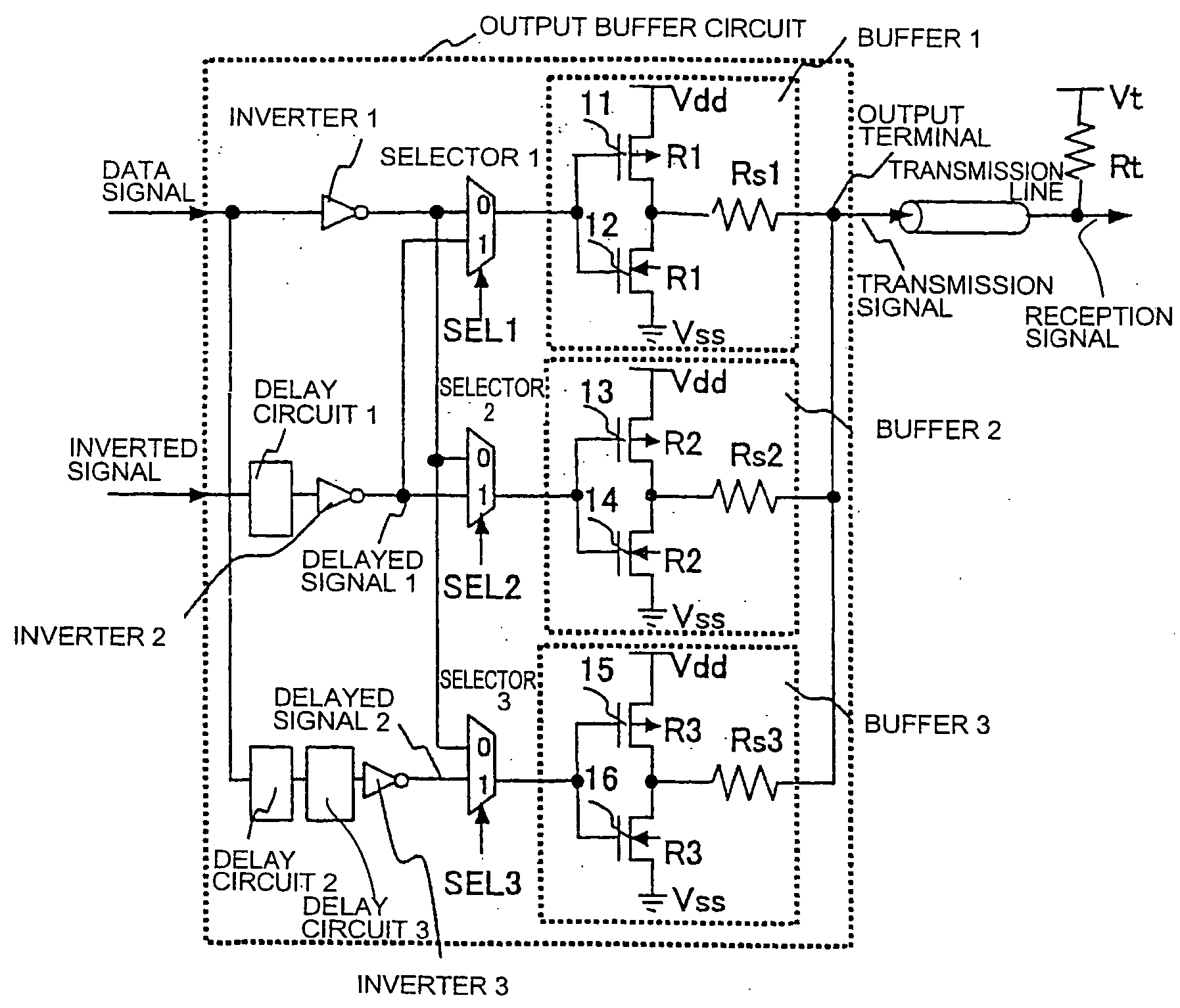
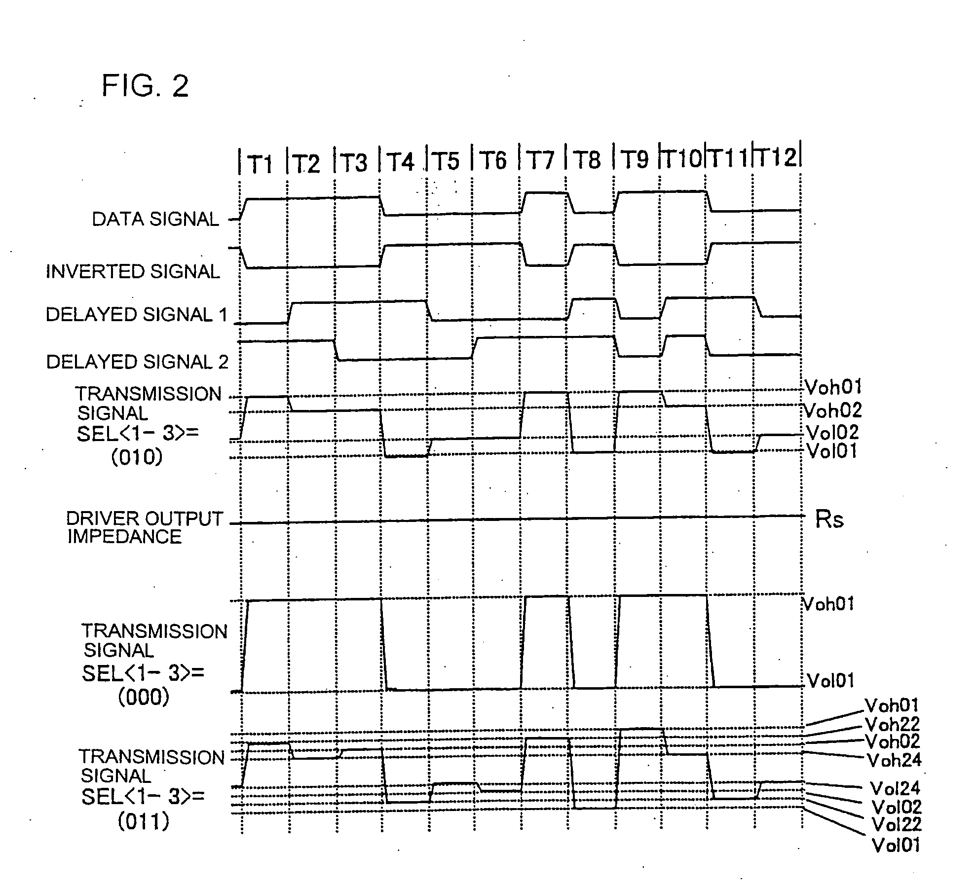
[0047]Example 1 will be explained. FIG. 1 is a configuration diagram illustrating circuitry according to Example 1 of the present invention. The output buffer according to Example 1 includes Buffer 1 to Buffer 3 that are connected in parallel with one another, selector logic for Selector 1 to Selector 3, Inverter 1 to Inverter 3, and Delay Circuit 1 to Delay Circuit 3. The output buffer receives a data signal and the inverted signal of the data signal and outputs a transmission signal to a transmission line connected to the output terminal.

[0048]The transmission line is connected at a reception terminal to a termination voltage Vt via a termination resistor Rt; the termination resistor Rt is made equal to the characteristic impedance of the transmission line so that no reflection wave is caused due to an impedance mismatch.

[0049]Inverter 1 receives a data signal having a logic value to be transmitted to the output terminal and outputs input signals for Selector 1 to Selector 3. Dela...

example 2

[0070]Example 2 will be explained. FIG. 3 is a configuration diagram illustrating circuitry according to Example 2 of the present invention. The output buffer according to Example 2 includes buffers 31 to 36 that are connected in parallel with one another, Inverter 1 to Inverter 3, and Delay Circuit 1 to Delay Circuit 3. The output buffer receives a data signal and the inverted signal of the data signal and outputs a transmission signal to a transmission line connected to the output terminal. The transmission line is connected at a reception terminal to a termination voltage Vt via a termination resistor Rt; the termination resistor Rt is made equal to the characteristic impedance of the transmission line so that no reflection wave is caused due to an impedance mismatch.

[0071]In Example 2, the objective, in which the output impedance of an output buffer circuit having an preemphasis function is made constant regardless of an adjustable preemphasis amount, the number of preemphasis t...

example 3

[0086]Example 3 will be explained. FIG. 5 is a circuit diagram illustrating the circuit configuration of a buffer according to Example 3 of the present invention. The configuration according to Example 3 is in such a way that part or all of Buffer 1 to Buffer 3 of the output buffer circuit according to Example 1 described above, or part or all of the buffers 31 to 36 of the output buffer circuit according to Example 2, each include the circuit illustrated in FIG. 5; the ON resistance of the buffer is made variable and the resistance value is enabled to be controlled by a voltage supplied from the outside of the buffer, so that the output impedance can be adjusted further flexibly.

[0087]In each of the buffers according to Example 3, a P-type transistor 51 and an N-type transistor 54 are connected between a high-potential power source Vdd and a low-potential power source Vss, and with the assistance of a signal applied to the input terminal, operate complementarily to each other; a P-...


PUM


Abstract

In an output buffer circuit including Inverter 1 to Inverter 3, Delay Circuit 1 to Delay Circuit 3 for delaying an input signal for a specific time, Buffer 1 to Buffer 3, and a function for transmitting a logic signal to a transmission path and in accordance with an amount of signal attenuation in the transmission path, creating at a transmission side a waveform including four or more kinds of signal voltages, the preemphasis amount is made variable and the ON resistance Rs of the buffer is made constant. Selector circuit 1 to Selector circuit 3 are situated before the buffers, the inverter, capable of selecting through selector logic a signal to be inputted to the buffer, inverts a data signal, and the preemphasis amount and the number of preemphasis taps are adjusted through a selection signal for the selector logic.

Description

[0001]The present application is based on and claims priority of Japanese patent application No. 2006-070415 filed on Mar. 15, 2006, the entire contents of which are hereby incorporated by reference.BACKGROUND OF THE INVENTION[0002]The present invention relates to an output buffer circuit for transmitting a logic signal to a transmission line, and more particularly to an output buffer circuit that has a function of applying preemphasis to a transmission-output waveform so as to compensate signal attenuation in a transmission line.[0003]The operating speeds of electronic circuit devices have been raised year after year, and research and development for realizing a higher-speed electronic circuit device have actively been performed. The realization of speedup of an electronic circuit device provides convenience in which, for example, processing that conventionally takes an extremely long time can be dealt with in a short time, or processing that has been thought to be impossible becom...

Claims


Application Information

Patent Timeline
Patent Type & Authority Applications(United States)
IPC IPC(8): H03K19/0185H03K19/0175
CPCH03K19/018521
Inventor MURAOKA, SATOSHICHUJO, NORIOORIHASHI, RITSURO
Owner HITACHI LTD
Why Eureka
Try Eureka