Tuning capacitance to enhance FET stack voltage withstand

a technology of capacitance and stack voltage, applied in the field of stacked transistor devices, can solve the problems of insufficient control signals of substantial amplitude, burdensome tradeoffs, and inability to manufacture transistors with higher bvds in the integrated circuit, and achieve the effect of effectively tuning the capacitance of the stack

Active Publication Date: 2008-10-30
PSEMI CORP
View PDF9 Cites 149 Cited by
  • Summary
  • Abstract
  • Description
  • Claims
  • Application Information

AI Technical Summary

Problems solved by technology

Integrated circuit fabrication requires many compromises.
In particular, many IC transistors that are otherwise highly effective for switching RF signals have a modest BVds, and thus may be inadequate to control signals of substantial amplitude.
However, the tradeoffs necessary to fabricate transistors with higher BVds in an integrated circuit may be burdensome.
For example, such design may be incompatible with other circuitry desired for the integrated circuit, or it may otherwise be uneconomical.
Thus, a stack of 10 transistors each having BVds of 1.8 V would ideally be capable of switching a signal having a peak amplitude of 18 V. In practice, unfortunately, such stacks may be unable to support such ideal voltage.
The voltage withstand capacity can be increased by increasing the number of devices in the stack, but this may cause large increases in the corresponding required integrated circuit area.
If eight transistors prove insufficient for this task in practice, then more transistors must be added to support the required voltage.
Unfortunately, the series resistance of the stack is the sum of the individual device resistances.
Moreover, the parasitic capacitances of these transistors typically increase with the area, and this can lead to numerous additional problems.
Research into observed failures of some stacked transistor RF switches at lower than expected applied switch voltages (Vsw) led to a conclusion that small parasitic capacitances (Cpd), previously thought negligible, were unexpectedly causing significant imbalances in the distribution of Vsw across the individual transistors of the stack.

Method used


Image

  • Tuning capacitance to enhance FET stack voltage withstand
  • Tuning capacitance to enhance FET stack voltage withstand
  • Tuning capacitance to enhance FET stack voltage withstand

Examples


Embodiment Construction

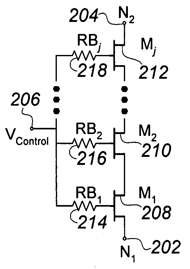
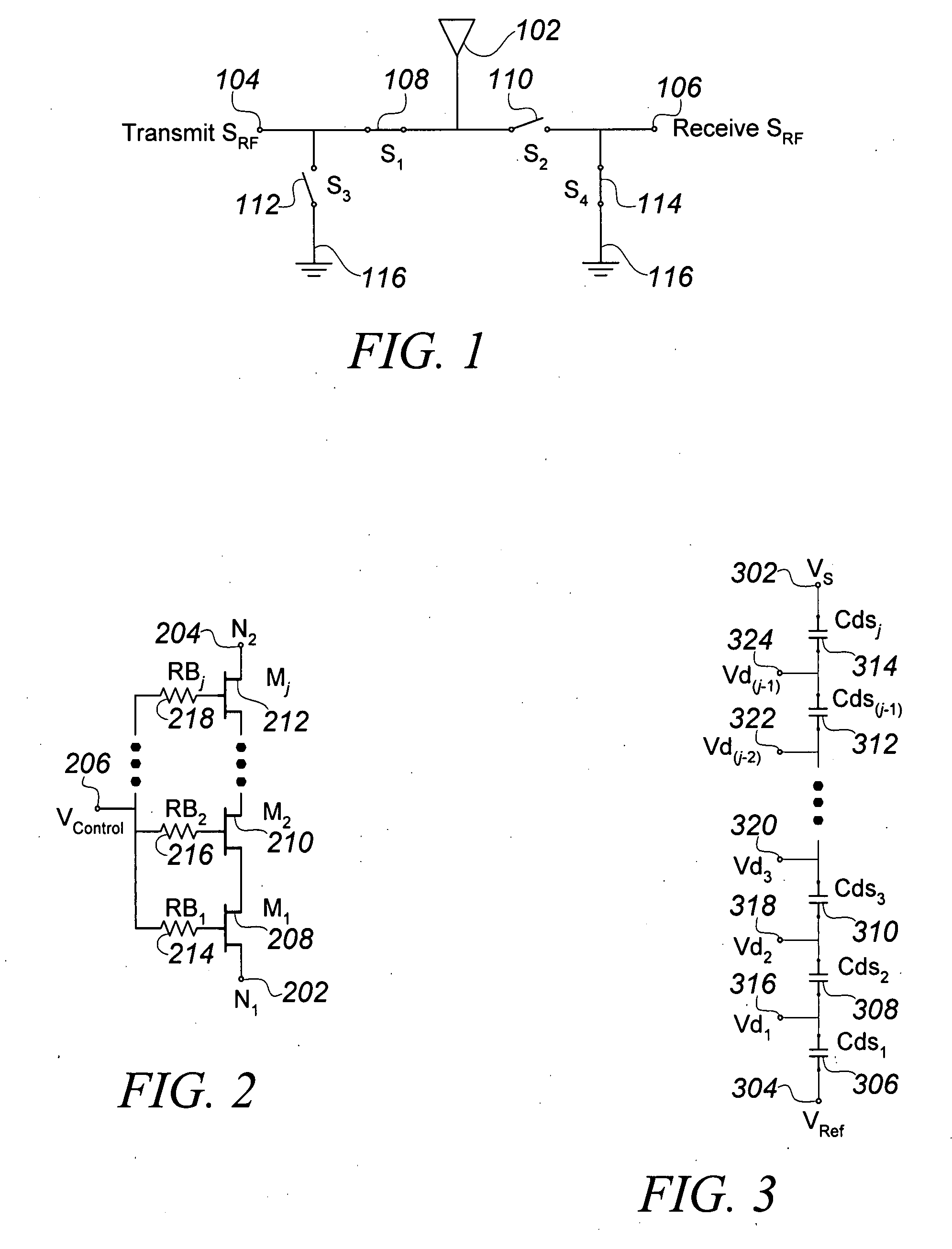
[0029]The background set forth above describes a typical stacked RF switch, as illustrated in FIG. 2. FIG. 3 illustrates how a switch such as shown in FIG. 2 should divide an applied RF voltage, such as (VS 302-VRef 304) such that equal voltages are imposed on each of the j FETs in the stack. When the switch is off (and presuming VRef is zero), VS 302 is applied to the endnodes 302-304 of the stack. Though each FET is in a high impedance state, the switch conducts somewhat due to the effective drain-source capacitances Cdsx corresponding to each FETE. Because the “off” conduction is almost entirely due to these capacitances, the FET structure itself is not shown, but only the j corresponding effective drain-source capacitances Cds1 306, Cds2 308, Cds3 310, . . . , Cds(j−1) 312 and Cdsj 314. This capacitive divider distributes the impressed voltage VS across each corresponding drain node to produce Vd1 316, Vd2 318, Vd3 320, . . . , Vd(j−2) 322 and Vd(j−1) 324.

[0030]If each Cdsx has ...


PUM

PropertyMeasurementUnit
drain-source capacitance Cdsaaaaaaaaaa
voltageaaaaaaaaaa
voltage V2aaaaaaaaaa

Abstract

An RF switch to controllably withstand an applied RF voltage Vsw, or a method of fabricating such a switch, which includes a string of series-connected constituent FETs with a node of the string between each pair of adjacent FETs. The method includes controlling capacitances between different nodes of the string to effectively tune the string capacitively, which will reduce the variance in the RF switch voltage distributed across each constituent FET, thereby enhancing switch breakdown voltage. Capacitances are controlled, for example, by disposing capacitive features between nodes of the string, and / or by varying design parameters of different constituent FETs. For each node, a sum of products of each significant capacitor by a proportion of Vsw appearing across it may be controlled to approximately zero.

Description

BACKGROUND[0001]1. Field[0002]The present disclosure relates to electronic integrated circuits (“ICs”), and more specifically to circuits comprised of stacked transistor devices for switching high frequency signals.[0003]2. Related Art[0004]Most radios, cell phones, TVs, and related equipment today require an “RF switch” to control connections between various transmitter and receiver circuits (“RF” is used generically herein to mean any reasonably high frequency ac signal). FIG. 1 is a simplified schematic diagram of a typical, simple two throw switch that may by used to switch, for example, a single antenna 102 between a transmit signal source 104 and a receive circuit 106. Switches S1 108, S2 110, S3 112 and S4 114 are represented by a mechanical single pole single throw switch symbol. Typically, the switches are controlled such that when S1 is “closed” or conducting at low impedance, S2 is “open” or high impedance. Because no switch is perfect, the node of a transmit / receive swit...

Claims


Application Information

Patent Timeline
Patent Type & Authority Applications(United States)
IPC IPC(8): H03K17/687
CPCH01H11/00H03K17/693Y10T29/49105H03K2017/066H03K17/161H03K17/6871H03K17/102
Inventor ENGLEKIRK, ROBERT MARK
Owner PSEMI CORP
Why Eureka
Try Eureka