
Vertical Type Nanotube Semiconductor Device

a semiconductor device, vertical type technology, applied in the direction of solid-state devices, transistors, nanoinformatics, etc., can solve problems such as electrical connection cutoff, and achieve the effect of improving adhesion and electrical connection

Inactive Publication Date: 2008-11-13
SAMSUNG ELECTRONICS CO LTD
View PDF3 Cites 40 Cited by
  • Summary
  • Abstract
  • Description
  • Claims
  • Application Information

AI Technical Summary

Benefits of technology

This approach prevents electrical cutoffs and improves integration density by maintaining conductivity and enhancing bonding strength between nanotube components, thereby ensuring reliable carrier migration and efficient device performance.

Problems solved by technology

However, if the bit line of several to several hundreds of nanometers is fabricated in a typical manner that simply decreases a width of a conductive material, then grain boundary defects within the bit line may cut off electrical connection.

Method used


Image

  • Vertical Type Nanotube Semiconductor Device
  • Vertical Type Nanotube Semiconductor Device
  • Vertical Type Nanotube Semiconductor Device

Examples


first embodiment

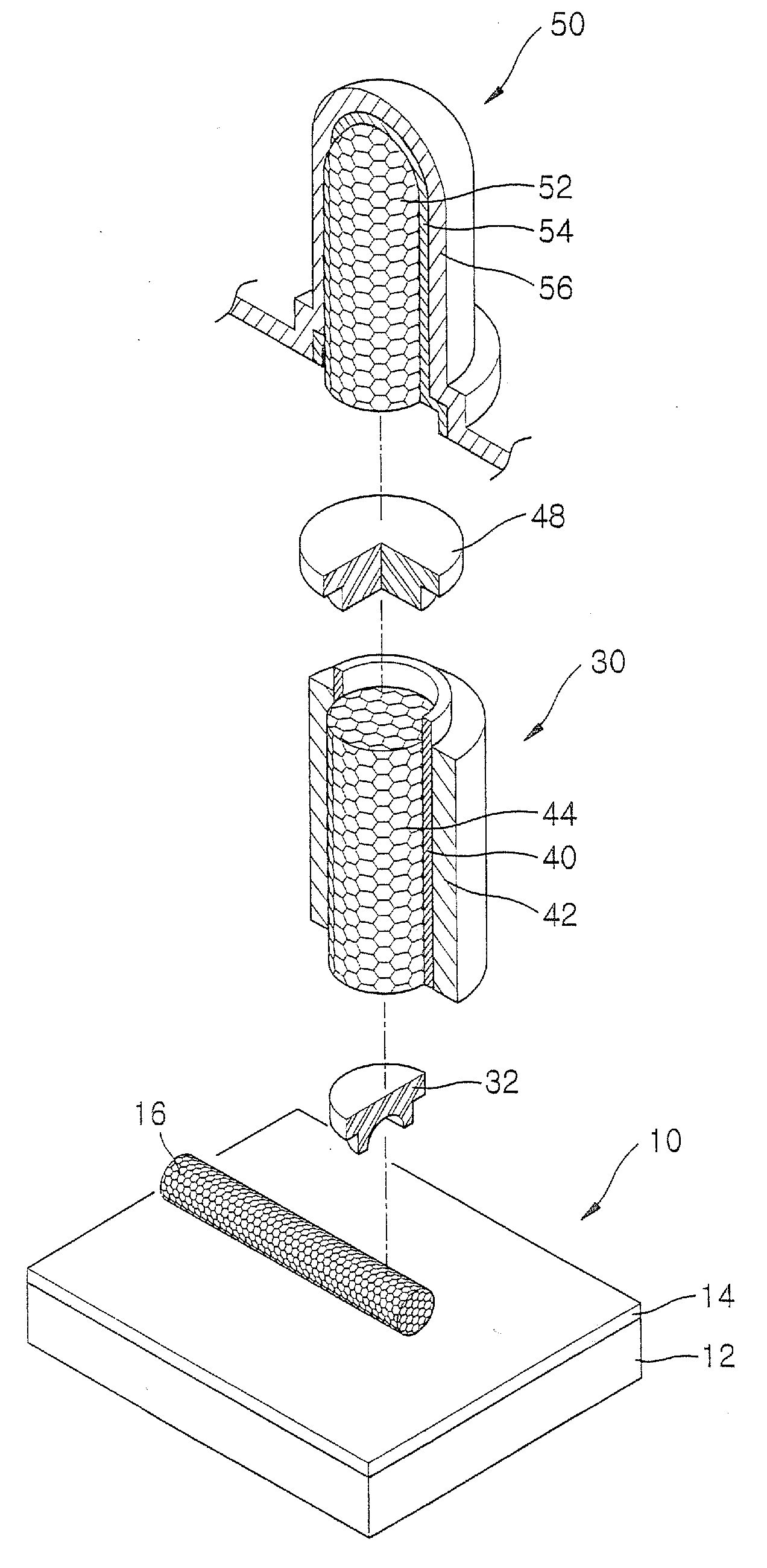
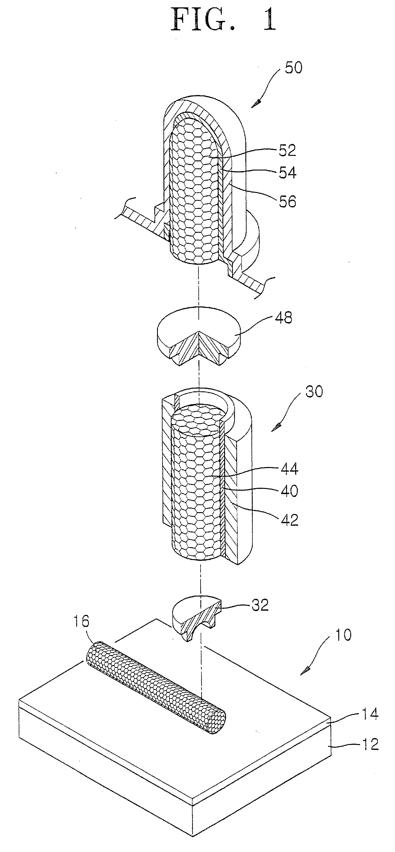
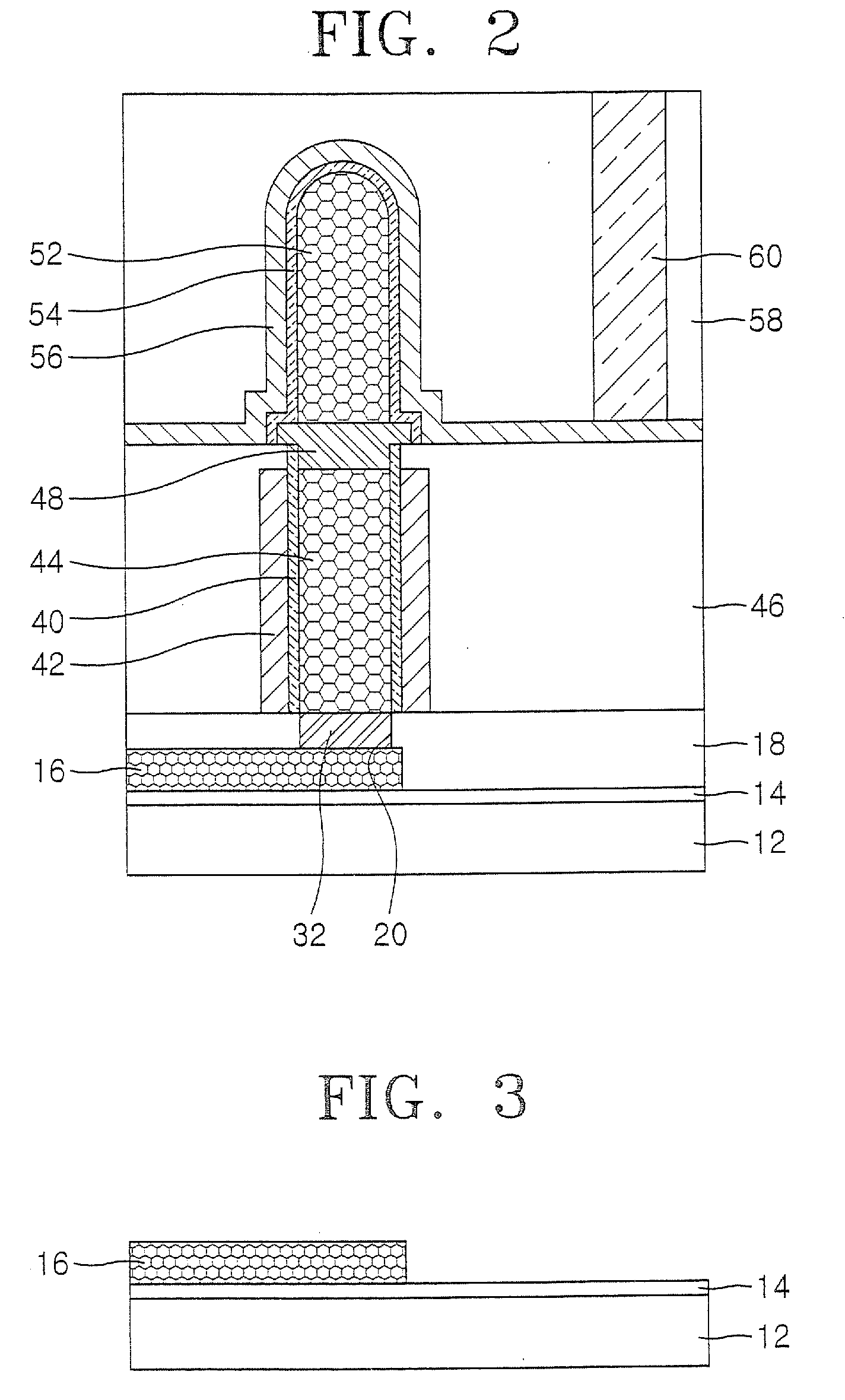
[0028]A nanotube semiconductor device according to the present invention has a vertical type structure. That is, a bit line formed on a substrate and an active region formed with a channel are arranged in the vertical direction with respect to the substrate. FIG. 1 is a perspective view of respective parts of a vertical type nanotube semiconductor device according to the present invention. FIG. 2 is a cross-sectional view showing major portions of FIG. 1. Referring to FIGS. 1 and 2, the vertical type nanotube semiconductor device includes a bit line part 10, a transistor part 30 and a capacitor part 50. The bit line part 10 includes a bit line 16 consisting of a nanotube with a conductive property disposed on a substrate 12 in parallel with the substrate 12. A first insulating layer 14 for electrical insulation may be disposed between the substrate 12 and the bit line 16. One end of the bit line 16 is connected to a recessed nanotube pole 44 extending vertically to the substrate 12....

second embodiment

[0046]FIG. 11 is an exploded perspective view of a vertical type nanotube semiconductor device according to the present invention. FIG. 12 is a cross-sectional view showing major portions of the device of FIG. 11. Referring to FIGS. 11 and 12, the vertical type nanotube semiconductor device is largely comprised of the bit line part 10, the transistor part 30, and the capacitor part 50. The bit line part 10 includes the bit line 16 consisting of the nanotube with the conductive property, and is disposed on the substrate 12 in parallel with the substrate 12. A first insulating layer 14 may be formed for electrical insulation between the substrate 12 and the bit line 16. The nanotube bit line 16 can be formed to have a nanometer dimension, and hardly has a grain boundary in the nanometer dimension, so that an electrical cutoff does not occur.

[0047]One end of the bit line 16 is connected to the recessed nanotube pole 44 extending in the vertical direction to the substrate 12. The recess...


PUM


Abstract

A vertical type nanotuhe semiconductor device including a nanotube bit line, disposed on a substrate and in parallel with the substrate and composed of a nanotube with a conductive property, and a nanotube pole connected to the bit line vertically to the substrate and provides a channel through which carriers migrate. By manufacturing the semiconductor device using the bit line composed of the nanotube, cutoff of an electrical connection of the bit line is prevented and an integration density of the semiconductor device can be improved.

Description

CROSS-REFERENCE TO RELATED APPLICATIONS[0001]This application is a continuation of U.S. patent application Ser. No. 11 / 325,964, filed on Jan. 5, 2006, which claims priority from Korean Patent Application No. 10-2005-0025368, filed on Mar. 28, 2005, the disclosures of both of which are incorporated herein by reference in their entiretyFIELD OF THE INVENTION[0002]The present invention relates to integrated circuit devices and, more particularly, to integrated circuit devices having nanotube conductive layers therein.BACKGROUND OF THE INVENTION[0003]Nanotubes with conductive properties are cylindrical members with highly microscopic diameters of several to several tens of nanometers and significantly large aspect ratios of about 10˜1,000. Carriers are migrated by ballistic transport within a nanotube having a generally uniform resistance along its length. Particularly, a carbon nanotube has carrier mobility of about 70 times or more than that of silicon at a room temperature.[0004]Beca...

Claims


Application Information

Patent Timeline
Patent Type & Authority Applications(United States)
IPC IPC(8): H01L29/06H01L29/94H10B12/00
CPCB82Y10/00H01L27/1085H01L27/10873H01L29/0665H01L29/0673H01L29/0676H01L29/78642H01L29/78681H01L29/7869Y10S977/938H10B12/03H10B12/05H01L21/18B82Y40/00
Inventor KIM, KI-NAMKIM, YUN-GI
Owner SAMSUNG ELECTRONICS CO LTD
Features
  • Generate Ideas
  • Intellectual Property
  • Life Sciences
  • Materials
  • Tech Scout
  • Unparalleled Data Quality
  • Higher Quality Content
  • 60% Fewer Hallucinations
Learn More