
High energy implant photodiode stack

a photodiode and high-energy technology, applied in the field of composite metal/oxide/semiconductor (cmos) imaging sensors, can solve the problems of reducing the spatial resolution of the imager sensor, the use of an external mechanical shutter for “still” shot imaging remains a problem, and the lack of isolation, etc., to achieve simple and cost-effective process integration and process integration. simple

Inactive Publication Date: 2008-11-13
SHARP KK
View PDF6 Cites 18 Cited by
  • Summary
  • Abstract
  • Description
  • Claims
  • Application Information

AI Technical Summary

Benefits of technology

The present invention provides a simple process integration method to fabricate vertically stacked photodiodes for R, G, and B light absorption and color imager fabrication. No silicon epitaxial layer is needed for the fabrication process, which reduces costs. An array of fully isolated multi-junction complimentary metal-oxide-semiconductor (CMOS) filterless color imager cells is provided, which includes a plurality of color imager cells formed in a bulk silicon substrate without an overlying epitaxial Si layer. The U-shaped well liner provides isolation between the photodiode sets, and each photodiode set includes a plurality of photodiodes and a U-shaped well liner bottom and walls that are p doped and electrically connected to a reference voltage. The method allows for the fabrication of cost-effective and efficient color imagers.

Problems solved by technology

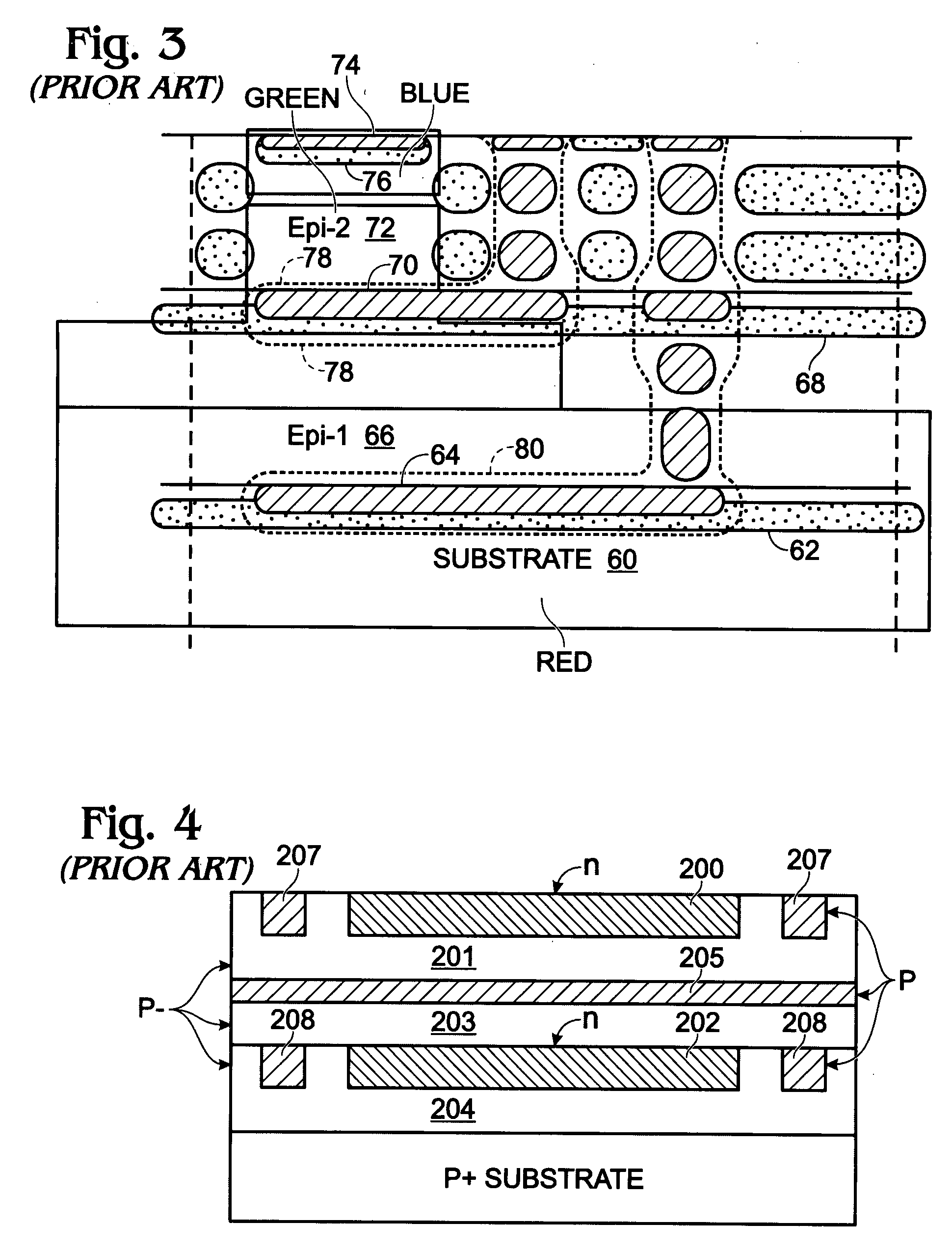
One problem associated with this structure is its complicated process steps.
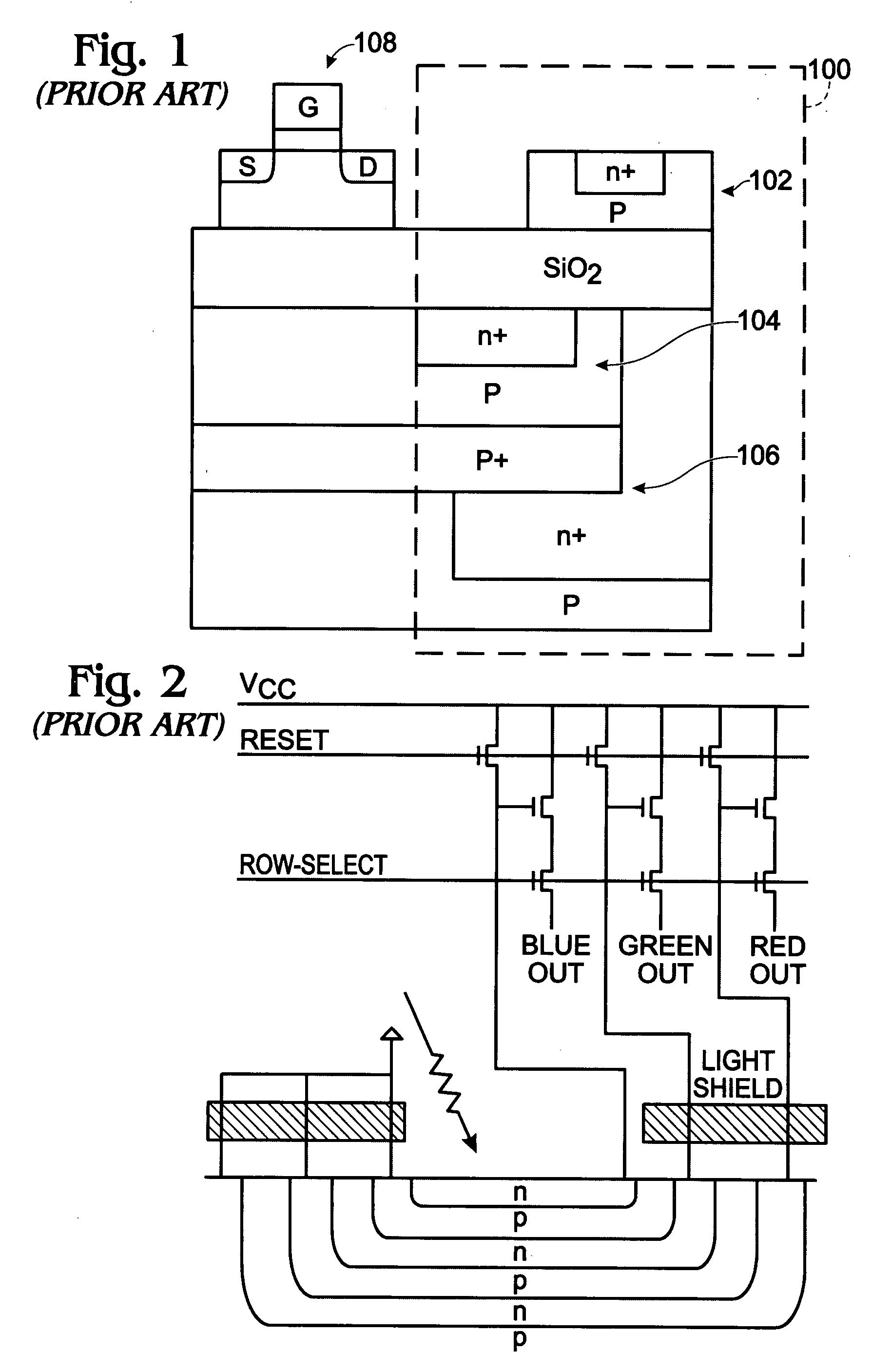
This lack of isolation decreases the spatial resolution of the imager sensor.
Therefore, the use of an external mechanical shutter for “still” shot imaging remains a problem.
Although BB—1 (Buried barrier) separates blue and green photon-generated electrons, and BB—2 separates green and red photon-generated electrons, there are no structures to completely prevent unintended electron flow through the substrate to neighboring red diode junctions.

Method used


Image

  • High energy implant photodiode stack
  • High energy implant photodiode stack
  • High energy implant photodiode stack

Examples


Embodiment Construction

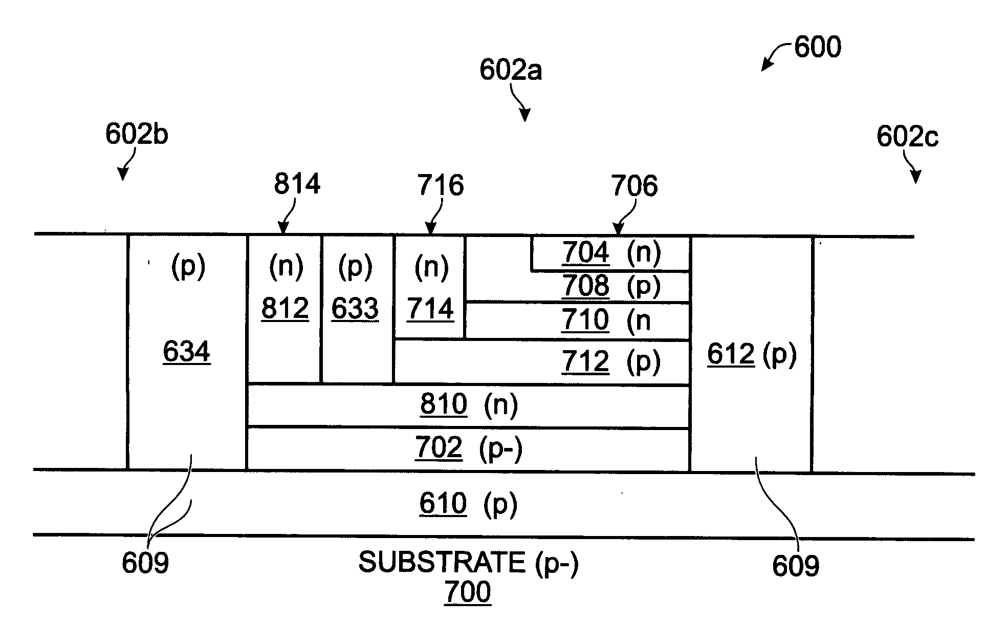
[0033]FIG. 6 is a partial cross-sectional view of an array 600 of fully isolated multi-junction complimentary metal-oxide-semiconductor (CMOS) filterless color imager cells 602. The color imager cell array 600 comprises a bulk silicon (Si) substrate 604 without an overlying epitaxial Si layer. A plurality of color imager cells are formed in the bulk Si substrate. Shown are cells 602a, 602b, and 602c. However, the array 600 is not limited to any particular number of cells. Although only three cells are shown, it should be understood that the array may be comprised of a much larger number cells configured in matrix, where each cell is identified by a position in a row and column. Although only a single cell from the array is detailed, it should be understood that the description of the cell (below) is applicable to every cell in the array.

[0034]Color imager cell 602a includes a photodiode set with a first photodiode, second photodiode, and third photodiode formed as a stacked multi-ju...


PUM


Abstract

An array of fully isolated multi-junction complimentary metal-oxide-semiconductor (CMOS) filterless color imager cells is provided, with a corresponding fabrication process. The color imager cell array is formed from a bulk silicon (Si) substrate without an overlying epitaxial Si layer. A plurality of color imager cells are formed in the bulk Si substrate, where each color imager cell includes a photodiode set and a U-shaped well liner. The photodiode set includes first, second, and third photodiode formed as a stacked multifunction structure, while the U-shaped well liner fully isolates the photodiode set from adjacent photodiode sets in the array. The U-shaped well liner includes a physically interfacing doped well liner bottom and first wall. The well liner bottom is interposed between the substrate and the photodiode set, and the first wall physically interfaces each doped layer of each photodiode in the photodiode set.

Description

BACKGROUND OF THE INVENTION[0001]1. Field of the Invention[0002]This invention generally relates to complementary metal / oxide / semiconductor (CMOS) imaging sensors and, more particularly, to a structure and associated fabrication process for using high energy ion implanting to form pixel diode sets and a well liner to isolate the photodiode sets in an array of photodiode sets.[0003]2. Description of the Related Art[0004]Silicon has characteristic photon absorption lengths that vary with the energy of the photons absorbed. For the wavelengths of 450 nanometers (nm), 550 nm, and 650 nm, the absorption lengths are 0.24 microns (μm), 1.13 μm, and 3.17 μm, respectively. This variation provides an opportunity to fabricate stacked diode junctions at depths that are capable of separating photons of various wavelengths, using standard CMOS manufacturing processes. Various technologies have been applied to this idea over the past 30 years and full color imaging is available in the market place...

Claims


Application Information

Patent Timeline
Patent Type & Authority Applications(United States)
IPC IPC(8): H01L31/113H01L31/18
CPCH01L27/1463H01L27/14647H01L27/14689
Inventor LEE, JONG-JANTWEET, DOUGLAS J.HSU, SHENG TENG
Owner SHARP KK
Learn More