Supercharge Your Innovation With Domain-Expert AI Agents!

Method and pad design for the removal of barrier material by electrochemical mechanical processing

Inactive Publication Date: 2008-11-13
APPLIED MATERIALS INC
View PDF10 Cites 5 Cited by
  • Summary
  • Abstract
  • Description
  • Claims
  • Application Information

AI Technical Summary

Problems solved by technology

This dichotomy of processing (e.g., Ecmp and CMP on a single system) requires divergent utilities and process consumables, resulting in higher cost of ownership.
Moreover, as most Ecmp processes utilize lower contact pressure between the substrate being processed and a processing surface, the heads utilized to retain the substrate during processing do not provide robust processing performance when utilized for conventional CMP processes, which typically have high contact pressures, which results in high erosion of conductive material disposed in trenches or other features.
As the removal rate of low pressure conventional CMP barrier layer processing is generally less than about 100 Å / min, conventional CMP processing of barrier materials using low pressure is not suitable for large scale commercialization.
However, because of the inertness of barrier materials, the removal current during Ecmp is very low.
Although the removal current can be increased by increasing the applied voltage, an applied voltage that is too high results in a very large leakage current between the contact materials.
This large leakage current results in poor contact between the substrate and the conductive pad materials.

Method used


Image

  • Method and pad design for the removal of barrier material by electrochemical mechanical processing
  • Method and pad design for the removal of barrier material by electrochemical mechanical processing
  • Method and pad design for the removal of barrier material by electrochemical mechanical processing

Examples


Embodiment Construction

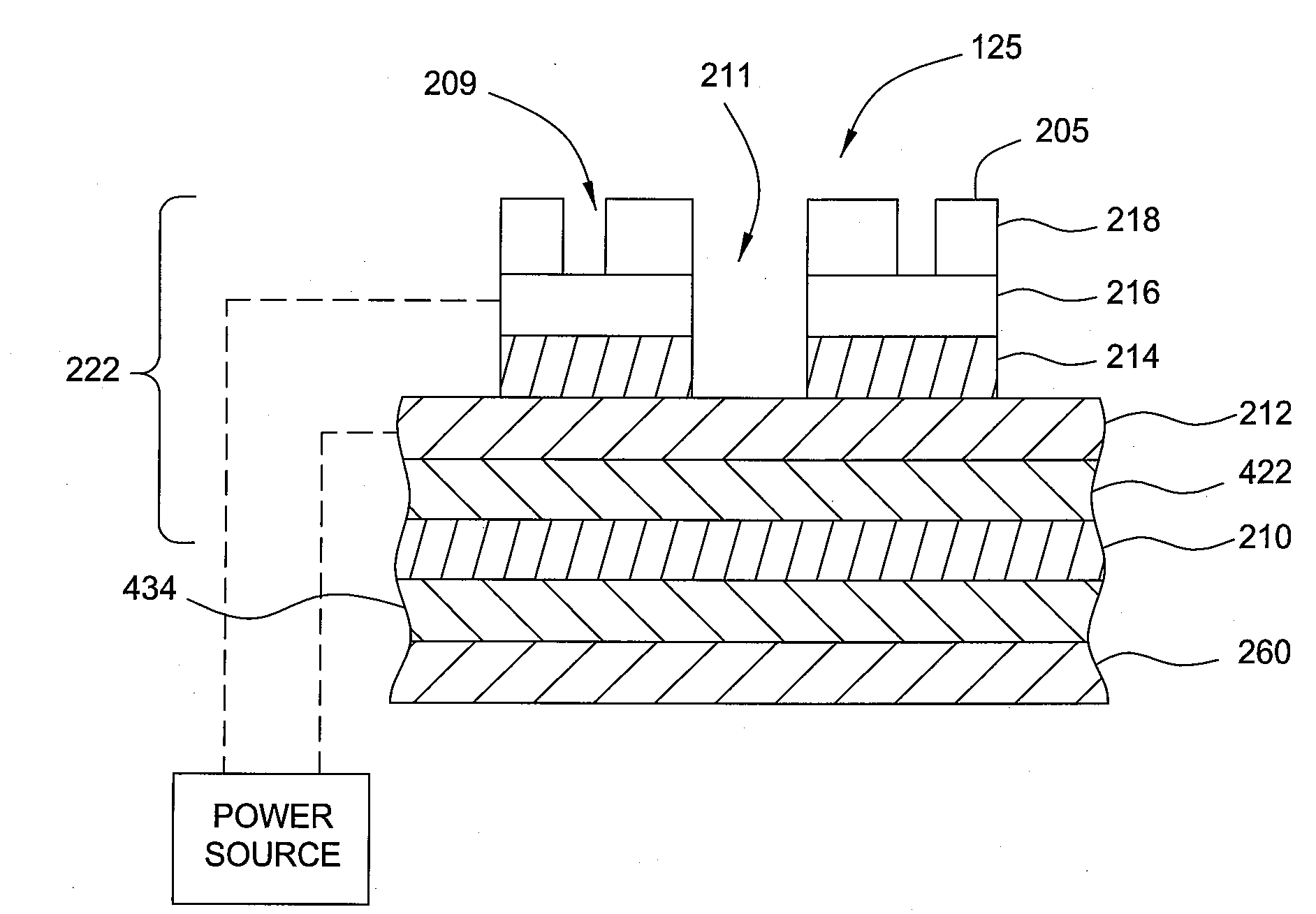
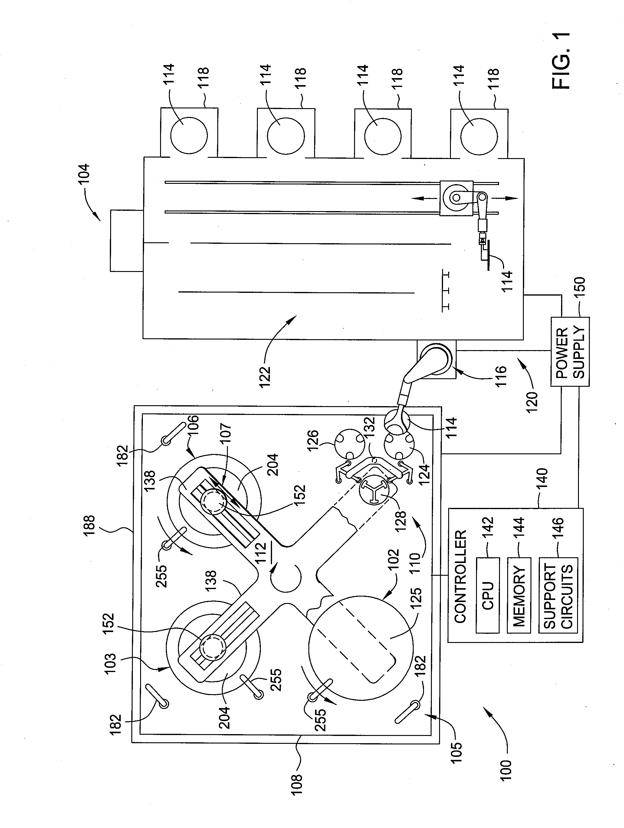
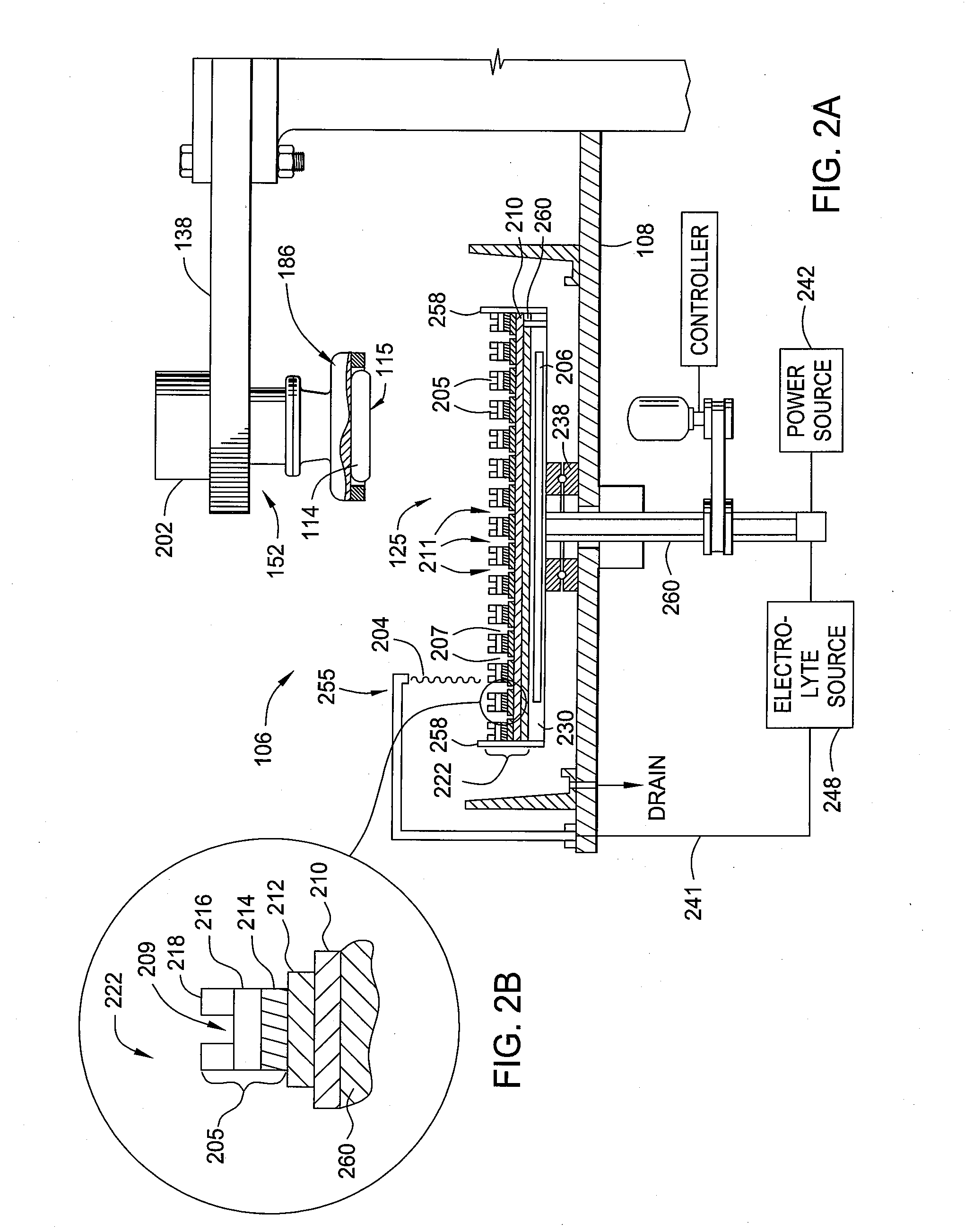
[0024]The words and phrases used in the present invention should be given their ordinary and customary meaning in the art by one skilled in the art unless otherwise further defined. Certain embodiments provide a method and processing apparatus for removal of conductive and barrier materials from a substrate.

[0025]As used herein, the term “electrochemical mechanical polishing” (Ecmp) generally refers to planarizing a substrate by the application of electrochemical activity, mechanical activity, and chemical activity to remove material from a substrate surface.

[0026]As used herein, the term “electropolishing” generally refers to planarizing a substrate by the application of electrochemical activity.

[0027]As used herein, the term “anodic dissolution” generally refers to the application of an anodic bias to a substrate directly or indirectly which results in the removal of conductive material from a substrate surface and into a surrounding polishing composition.

[0028]As used herein, the...


PUM

PropertyMeasurementUnit
Thicknessaaaaaaaaaa
Thicknessaaaaaaaaaa
Electric potential / voltageaaaaaaaaaa

Abstract

A method and apparatus for processing barrier and metals disposed on a substrate in an electrochemical mechanical planarizing system are provided. In certain embodiments a method for electroprocessing a substrate is provided. The method comprises contacting the substrate with the non-conductive surface of a polishing pad assembly, establishing a first electrically conductive path through an electrolyte between an exposed layer of barrier material and a first electrode, establishing a second electrically conductive path through the electrolyte between the exposed layer of barrier material and a second electrode, applying a voltage to the first electrode to cause a voltage drop between the substrate and the second electrode, and removing the barrier material from the substrate.

Description

BACKGROUND OF THE INVENTION[0001]1. Field of the Invention[0002]Embodiments of the present invention as recited by the claims generally relate to a method and processing apparatus for planarizing or polishing a substrate. More particularly, the invention relates to a method and a polishing pad for planarizing or polishing a semiconductor substrate by electrochemical mechanical polishing.[0003]2. Description of the Related Art[0004]In the fabrication of integrated circuits and other electronic devices on substrates, multiple layers of conductive, semiconductive, and dielectric materials are deposited on or removed from a substrate, such as a semiconductor wafer. As layers of materials are sequentially deposited and removed, the substrate may become non-planar and require planarization, in which previously deposited material is removed from the substrate to form a generally even, planar or level surface. The process is useful in removing undesired surface topography and surface defect...

Claims


Application Information

Patent Timeline
IPC IPC(8): H01L23/485H01L21/4763
CPCB23H5/08H01L21/32125
Inventor LIU, FENG Q.DUBOUST, ALAINWANG, YANHSU, WEI-YUNGDU, TIANBO
Owner APPLIED MATERIALS INC
Features
  • R&D
  • Intellectual Property
  • Life Sciences
  • Materials
  • Tech Scout
  • Unparalleled Data Quality
  • Higher Quality Content
  • 60% Fewer Hallucinations
Learn More