Method for manufacturing a field effect transistor having a field plate

a field electrode and transistor technology, applied in the direction of basic electric elements, electrical appliances, semiconductor devices, etc., can solve the problem that oxygen is not used for etching the insulating film, and achieve the effect of high adhesiveness

Inactive Publication Date: 2008-11-20
OKI ELECTRIC IND CO LTD
View PDF2 Cites 123 Cited by
  • Summary
  • Abstract
  • Description
  • Claims
  • Application Information

AI Technical Summary

Benefits of technology

[0016]It is an object of the present invention to provide a GaN-based FET that has a high adhesiveness between a field plate and an insul

Problems solved by technology

Therefore, oxygen is not used f

Method used


Image

  • Method for manufacturing a field effect transistor having a field plate
  • Method for manufacturing a field effect transistor having a field plate
  • Method for manufacturing a field effect transistor having a field plate

Examples


Embodiment Construction

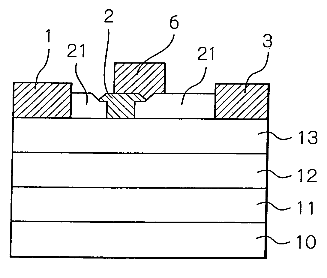
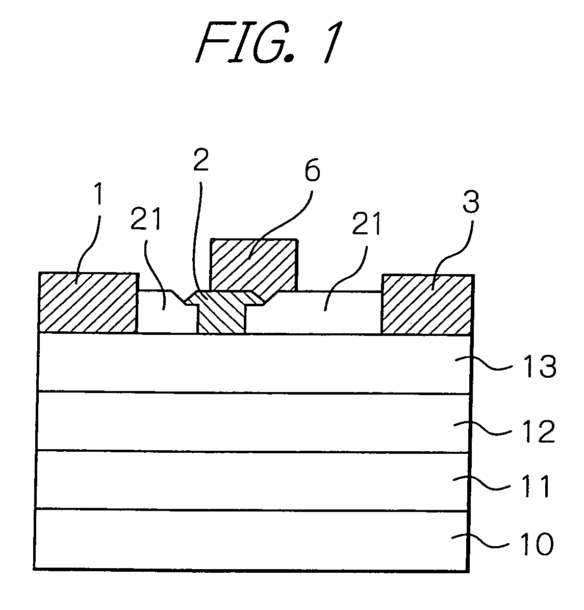
[0025]A preferred embodiment in accordance with the present invention will be described below with reference to the accompanying drawings. Since the drawings are merely for illustration, the present invention is not to be restricted by what are shown in the drawings. Specifically, those drawings are simplified schematic representations intended to generally illustrate the shape, size, and positional relationships of the various structural components to the extent that the present invention can be understood by those skilled in the art. For the purpose of better understanding, the figures are drawn with some dimensions exaggerated. Further, preferred exemplary configurations of the invention will be given below. However, the materials used, numerical conditions and so forth given below are nothing but examples in the scope included in the essence of the invention.

[0026]FIG. 1 is a schematic block diagram showing a field effect transistor (FET) in accordance with an embodiment of the ...


PUM


Abstract

An opening for forming a gate electrode is provided by a first photoresist pattern formed on an insulating film. Reactive ion etching by inductively coupled plasma is applied to the insulating film through the first photoresist pattern as a mask to thereby expose the surface of a GaN semiconductor layer, evaporating thereon a gate metal such as NiAu, thereby forming the gate electrode by self-aligned process. This prevents an oxidized film from being formed on the surface of the semiconductor layer. After the gate electrode is formed, a second photoresist pattern is formed to form a field plate on the gate electrode and the insulating film through the second photoresist pattern as a mask. Thereby, Ti having a high adhesiveness with an insulating film made of SiN or the like can be used as a field plate metal.

Description

BACKGROUND OF THE INVENTION[0001]1. Field of the Invention[0002]The present invention relates to a method for manufacturing a field effect transistor (FET) having a gate electrode, such as a GaN-based FET having a gate electrode for use in a power amplifier.[0003]2. Description of the Background Art[0004]In an FET for use in a power amplifier required to have a high breakdown voltage, a field plate is often provided in its gate electrode to relax electric field concentration in the drain electrode side end portion of the gate electrode, thereby reducing Schottky reverse leakage and improving a drain breakdown voltage.[0005]FIG. 2 shows a conventional FET having a field plate disclosed in U.S. patent application publication No. 2006 / 0102929 A1 to Okamoto et al. This FET has a cross-sectional structure shown in FIG. 2, including an undoped GaN semiconductor layer having a buffer layer 11, a channel layer 12, and an electron supply / Schottky barrier layer 13 formed on a substrate 10 in ...

Claims


Application Information

Patent Timeline
IPC IPC(8): H01L29/778H01L21/338
CPCH01L29/2003H01L29/402H01L29/42316H01L29/66462H01L29/7787
Inventor HOSHI, SHINICHIITOH, MASANORIOKITA, HIDEYUKIMARUI, TOSHIHARU
Owner OKI ELECTRIC IND CO LTD
Why Eureka
Try Eureka