Apparatus and Methods for Constructing Semiconductor Chip Packages with Silicon Space Transformer Carriers

Inactive Publication Date: 2008-11-20
IBM CORP
View PDF10 Cites 179 Cited by
  • Summary
  • Abstract
  • Description
  • Claims
  • Application Information

AI Technical Summary

Benefits of technology

[0007]Exemplary embodiments of the invention generally include apparatus and methods for high density packaging of semiconductor chips using silicon space transformer chip level package structures, which allow high density chip interconnection and/or integration of multiple chips or chip stacks

Problems solved by technology

SoC solutions may not be practical or achievable for chip-level integration when given systems design requires the use of heterogeneous semiconductor technologies to fabricate the necessary system integrated circuits.
In addition, when fabricating thinned IC devices, packages, IC stacks or package stacks, the thinned components may be fragile to handle and lead to yield losses if broken or damaged and may become non planar due to stresses such as circuits, wiring or vias causing the thinned component to bend or bow.
In some cases, the bow or bending can foe excessive and make handling or assembly difficult or impossible without added costs of mechanical hand

Method used


Image

  • Apparatus and Methods for Constructing Semiconductor Chip Packages with Silicon Space Transformer Carriers
  • Apparatus and Methods for Constructing Semiconductor Chip Packages with Silicon Space Transformer Carriers
  • Apparatus and Methods for Constructing Semiconductor Chip Packages with Silicon Space Transformer Carriers

Examples


Embodiment Construction

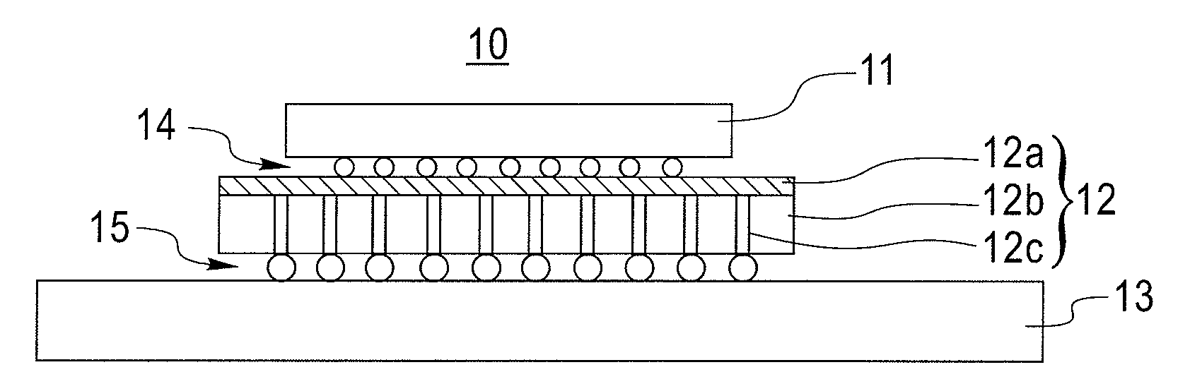
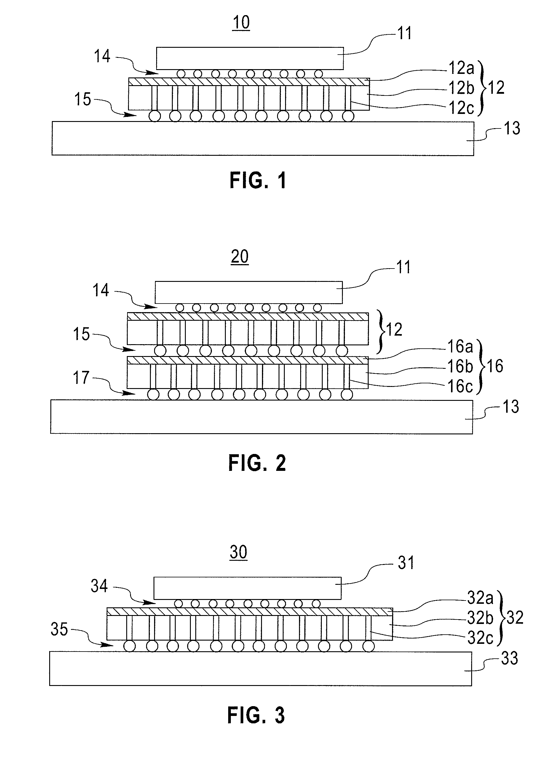
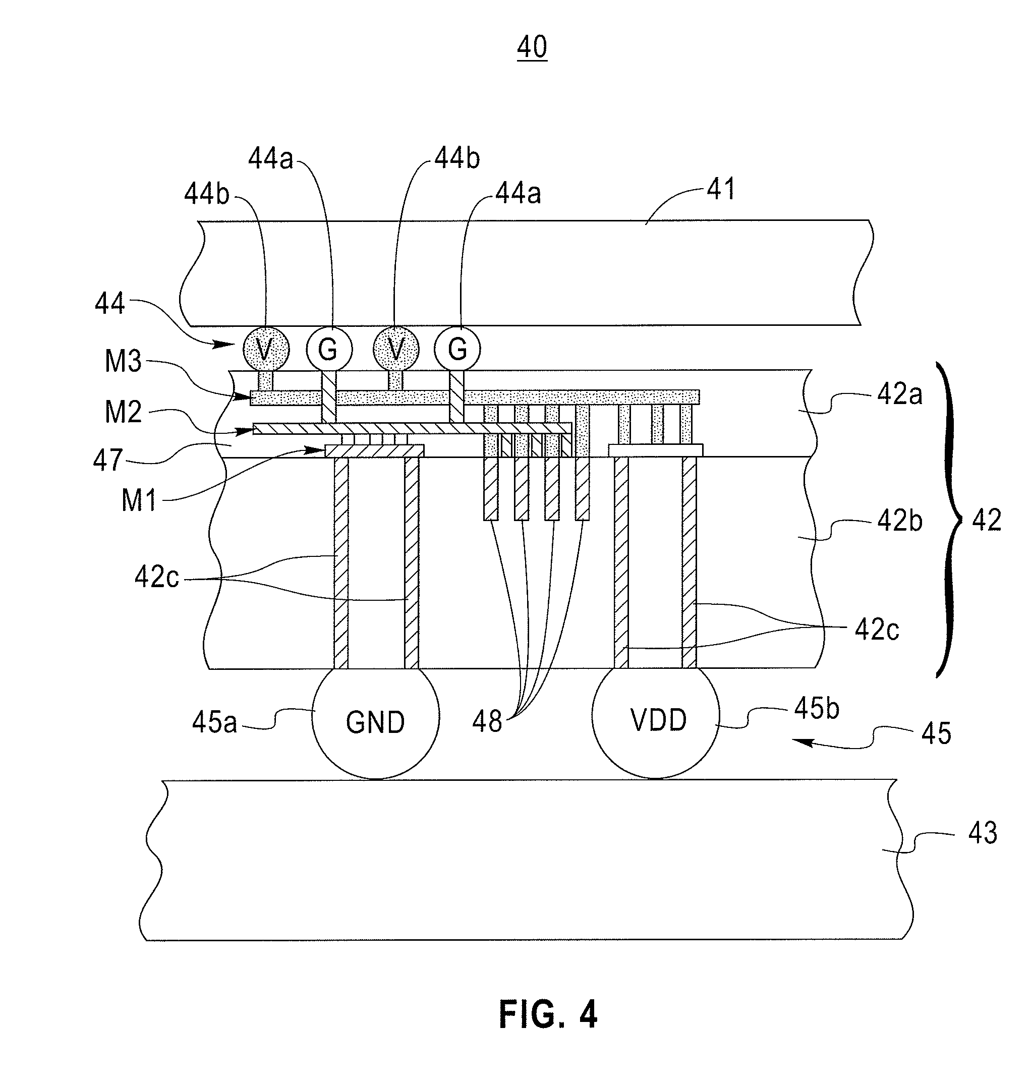
[0025]Exemplary embodiments of the invention as discussed herein generally include apparatus and methods for high density packaging of semiconductor chips using silicon space transformer chip level package structures. For instance, FIGS. 1˜4 and 5A˜5C are high-level schematic illustrations of various chip package structures in which high-density chip level packaging may be realized using one or more thinned silicon space transformer substrate layers. As explained in further detail below, silicon space transformer package structures according to exemplary embodiments of the invention may utilize state of the art silicon manufacturing techniques which follow CMOS back-end-of line design rules to realize low-cost fabrication of silicon space transformer package structures having high density wiring and conductive through-via interconnects which provide space transformation using one or more thinned silicon space transformer substrate layers for high I / O density packaging of one or more...


PUM


Abstract

Apparatus and methods are provided for high density packaging of semiconductor chips using silicon space transformer chip level package structures, which allow high density chip interconnection and/or integration of multiple chips or chip stacks high I/O interconnection and heterogeneous chip or function integration.

Description

GOVERNMENT LICENSE RIGHTS[0001]This invention was made with Government support under Contract No. H98230-04-C-0920, NBCH3039004 awarded by the DARPA (Defense Advanced Projects Agency) The Government has certain rights in this invention.TECHNICAL FIELD OF THE INVENTION[0002]The present invention relates generally to microelectronic packaging of semiconductor chips and, more specifically, apparatus and methods for high density packaging of semiconductor chips using silicon space transformer chip level package structures.BACKGROUND[0003]Advances in semiconductor chip fabrication and packaging technologies have enabled the development of highly integrated semiconductor chips and compact chip package structures or electronic modules. For example, silicon integrated circuit chips can be fabricated with high integration density and functionality to form what is referred to as SoC (System on Chip). With SoC designs, the functionality of a complete system (e.g., computer) is integrated on a ...

Claims


Application Information

Patent Timeline
IPC IPC(8): H01L23/48H01L21/00
CPCH01L21/6835H01L23/147H01L23/49827H01L23/49833H01L23/50H01L24/81H01L25/0655H01L25/0657H01L2221/68345H01L2224/81801H01L2924/01077H01L2924/01079H01L2924/15174H01L2924/15311H01L2924/19041H01L2924/3025H01L2224/16225H01L2924/01019H01L2924/10253H01L2924/00H01L2924/19011H01L2924/19042H01L2924/19043H01L2924/14H01L2924/00014H01L2924/00011H01L21/76898H01L2224/0401
Inventor ANDRY, PAUL S.COTTE, JOHN M.KNICKERBOCKER, JOHN U.TSANG, CORNELIA K.
Owner IBM CORP
Why Eureka
Try Eureka