

Mems Filter Device and Manufacturing Method Thereof
a filter device and filter technology, applied in the direction of electrical equipment, material nanotechnology, nanotechnology, etc., can solve the problems of inability to obtain the desired passband waveform, and achieve the effects of reducing cost, reducing cost, and flexible design of filter q value and frequency bandwidth
- Summary
- Abstract
- Description
- Claims
- Application Information
AI Technical Summary
Benefits of technology
Problems solved by technology
Method used
Image

Examples
first embodiment
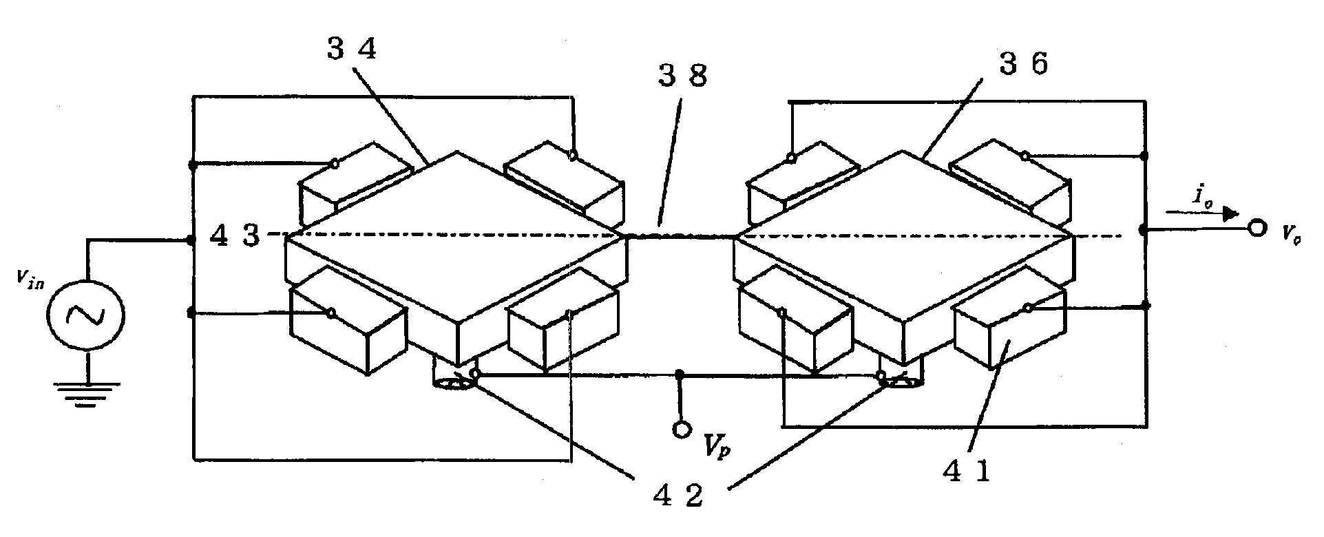
[0128]Next, a first embodiment of the invention will be discussed. FIG. 1 is a perspective view to show a MEMS filter unit of the first embodiment of the invention, and the MEMS filter unit is joined according to a first coupling method of MEMS filter. Components identical with those in FIG. 1 are denoted by the same reference numerals in FIGS. 2 and 3 and will not be discussed again.
[0129]The MEMS filter unit is characterized by the fact that first and second MEMS resonators 34 and 36 are joined by a first coupling element 38 implemented as a CNT, as shown in FIG. 1. The first and second MEMS resonators 34 and 36 have the same structure and each form a quadrilateral resonating body and are mechanically connected by the first coupling element 38, as shown in FIG. 1. A cylindrical column 42 is connected to the center of each MEMS resonator. It serves as a post for supporting the structure 34 and 36, and is joined to a substrate not shown.
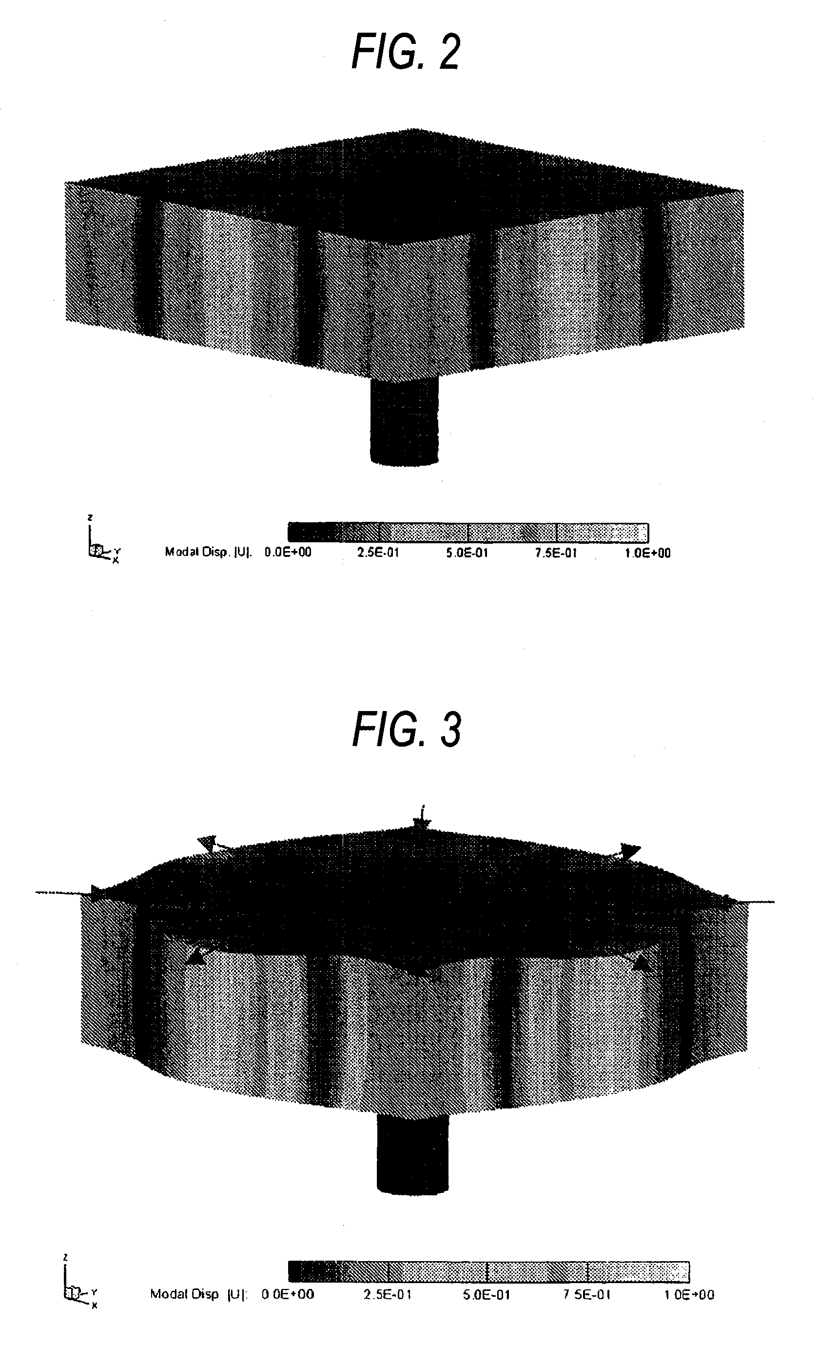
[0130]The dimensions of each of the MEMS reson...
second embodiment
[0158]Next, a second embodiment of the invention will be discussed.
[0159]The post 42 in the first embodiment of the invention is made of polysilicon; in the second embodiment, an example wherein the portion corresponding to the post 42 is formed of CNT 12 will be discussed.
[0160]The embodiment is characterized by a hole previously formed in the portion corresponding to a node of a resonating body and CNT grown in the hole by self-assembly; and a connection part of the resonating body is filled with polysilicon, etc., to provide strong connection.
[0161]FIGS. 17 to 22 show the manufacturing process represented as the section corresponding to the section taken on the dashed line 43 in FIG. 1. FIG. 17 shows a state before removal of the sacrifice layer 110 using photoresist as a mask to form trenches 96, which is equivalent to step in FIG. 5.
[0162]Catalysts 106 are formed according to a vacuum evaporation method (FIG. 18). In the example, an evaporator is used to avoid deposition on sid...
third embodiment
[0169]FIG. 23 shows a second coupling method of MEMS filter in a third embodiment of the invention. Components identical with those in FIG. 23 are denoted by the same reference numerals in FIGS. 24, 25, and 26 and will not be discussed again.
[0170]The embodiment is characterized by the fact that center parts corresponding to coupling nodes of first and second MEMS resonators 70 and 72 each having a quadrilateral shape are connected mechanically by a first coupling element 74 implemented as CNT, as shown in FIG. 23. Others are similar to those of the first embodiment shown in FIG. 1 and a fixed electrode 76 of each MEMS resonator is shown.
[0171]As a manufacturing method, a method corresponding to the second coupling method described above is adopted for forming resonating bodies of the first and second MEMS resonators 70 and 72 and then joining them by the coupling element 74.
[0172]It is assumed that the MEMS resonator resonant mode in the first embodiment is used as a resonant mode....
PUM
 Abstract
Description
Claims
Application Information