Image sensor and an electronic information device

a technology which is applied in the field of image sensor and electronic information device, can solve the problems of increasing chip size, reduce the negative effect of reset voltage, suppress the increase in chip size, and reduce the dispersion of unnatural colors in the high luminance subject in the display image

Active Publication Date: 2008-11-20
SHARP KK
View PDF1 Cites 12 Cited by
  • Summary
  • Abstract
  • Description
  • Claims
  • Application Information

AI Technical Summary

Benefits of technology

[0047]The present invention is intended to solve the conventional problems described above. The objective of the present invention is to obtain an image sensor and an electronic information device using such image sensor which is capable of avoiding a phenomenon of the blackening of the high luminance subject while suppressing the increase in the chip size and the dispersion of natural colors in the high luminance subject.
[0071]By having the gate length of the read transistor for supplying the second reset current which constitutes the reset current supply section being longer than the gate length of the read transistor for supplying the first reset current which constitutes the pixel, the dispersion of color in the high luminance subject due to the manufacturing dispersion of the transistor threshold value in the reset current supply section can be even more alleviated.

Problems solved by technology

However, this is a typical problem caused by an image sensor having a correlated double sampling circuit which outputs the difference between the reset voltage and the signal voltage as a photo-detection signal (pixel signal).
When adding the control circuit for each read line, it leads to an increase in chip size.

Method used


Image

  • Image sensor and an electronic information device
  • Image sensor and an electronic information device
  • Image sensor and an electronic information device

Examples


embodiment 1

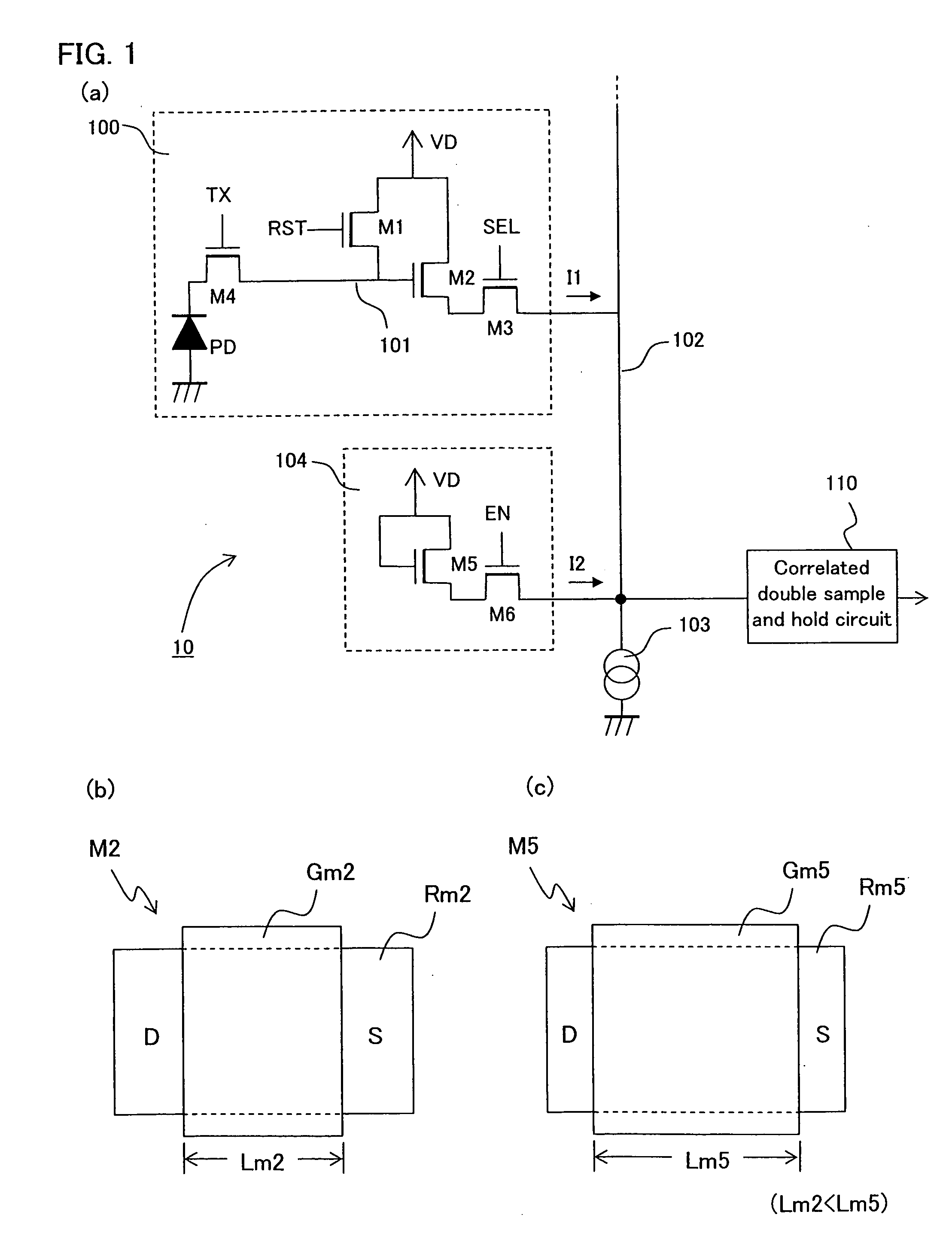
[0105]FIG. 1 is a diagram describing an image sensor of the Embodiment 1 of the present invention, in which FIG. 1(a) shows a circuit configuration of a pixel and a circuit configuration of a reset current supply section in the image sensor, FIG. 1(b) shows a gate length of the read transistor constituting the pixel, and FIG. 1(c) shows a gate length of the read transistor in the reset current supply section.

[0106]The pixel 100 constituting the image sensor 10 of the present Embodiment 1 has a four-transistor configuration. That is, the pixel 100 comprises a photo diode PD for converting light into electrons, a transmission transistor M4 for transmitting the charge generated at the photo diode PD wherein the TX signal is input to the gate, a read transistor M2 for amplifying the level of the charge and generating the signal voltage corresponding thereto, a reset transistor M1 for resetting the gate 101 of the read transistor M2 to the VD voltage, i.e., the high potential voltage (fo...

embodiment 2

[0147]FIG. 4 is a diagram describing an image sensor of the Embodiment 2 of the present invention, in which FIG. 4(a) shows a configuration of a pixel and a configuration of a reset current supply circuit in the image sensor, and FIG. 4(b) schematically shows a shaded region in the pixel array of the image sensor.

[0148]The image sensor 10a of the Embodiment 2 uses a dummy pixel 10a instead of the reset current supply circuit 104 in the image sensor 10 of Embodiment 1.

[0149]That is, in the image sensor in the Embodiment 2, as shown in FIG. 4(b), pixels for one row located in the shaded area 11a at the upper part or the lower part of the space is used as the reset current supply circuit for supplying the reset current to each read line. Moreover, 11b in the diagram is a light receiving part of an image sensor in the unshaded pixel column area.

[0150]This dummy pixel 100a, similar to the pixel 100, comprises a photo diode PDa, a reset transistor M1a, a read transistor M2a, a selecting t...

embodiment 3

[0152]FIG. 5 is a diagram describing an image sensor of the Embodiment 3 of the present invention, in which the diagram shows a configuration of a pixel and a configuration of a reset current supply circuit in the image sensor.

[0153]The image sensor 10b of the Embodiment 3, similar to the image sensor 10a of the Embodiment 2, uses a dummy pixel 100b located in the shaded portion of the pixel array instead of the reset current supply circuit 104 in the image sensor 10 of Embodiment 1. However, in the dummy pixel 100b in this Embodiment 3, the elements are not formed in the area where the transmission transistor M4 and the photo diode PD are to be formed in the pixel.

[0154]That is, the dummy pixel 10b comprises a reset transistor M1b, a read transistor M2b and a selecting transistor M3b. In this dummy pixel 100b, similar to the dummy pixel 100a of the Embodiment 2, the gate of the reset transistor M1b is connected to the VD source, and an EN signal which is a control signal at an H le...


PUM


Abstract

An image sensor is disclosed. The image sensor includes a plurality of pixels arranged in a matrix which detects a pixel signal of each pixel based on a voltage difference between a reset voltage which is a reference voltage of each pixel and a signal voltage generated by a photoelectric conversion at each pixel, and includes a plurality of read lines located for each pixel column, wherein the reset voltage and the signal voltage are read from the pixel of the corresponding pixel column; and a reset current supply section provided for each read line, wherein at the same time a first reset current is supplied from a pixel to the read line when reading the reset voltage from the pixel, the section supplies a second reset current to the read line such that a sum of the first reset current and the second reset current is constant.

Description

[0001]This Nonprovisional Application claims priority under 35 U.S.C. §119(a) on Patent Application No. 2007-131071 filed in Japan on May 16, 2007, the entire contents of which are hereby incorporated by reference.BACKGROUND OF THE INVENTION[0002]1. Field of the Invention[0003]The present invention relates to an image sensor and an electronic information device, particularly to an improvement in quality of locally bright images such as sunlight and the like. The present invention can be applied to a pixel read circuit such as of a CMOS image sensor used in an electronic image capturing device such as a video camera, a digital camera and the like.[0004]2. Description of the Related Art[0005]FIG. 8 is a diagram describing a conventional image sensor. This diagram shows one pixel in an image sensor and a circuit holding a signal value read from the pixel. FIG. 9 is a timing chart describing the operation of a conventional image sensor.[0006]A pixel 200 constituting the conventional ima...

Claims


Application Information

Patent Timeline
Patent Type & Authority Applications(United States)
IPC IPC(8): H04N5/335H04N5/217H01L27/146H04N5/355H04N5/357H04N5/369H04N5/374H04N5/376
CPCH04N3/1568H04N5/3598H04N5/374H04N25/627H04N25/76H04N25/65H04N25/75
Inventor HATTORI, SHINJI
Owner SHARP KK
Why Eureka
Try Eureka