Method For Manufacturing Epitaxial wafer

a manufacturing method and technology of epitaxial wafers, applied in the field of epitaxial wafer manufacturing, can solve the problems of reducing the life of the device, increasing the leak current or the decrease of the lifetime of the device, and complicated process, so as to prevent the generation of excessive amounts of oxygen precipitate nuclei, reduce the rejection rate, and suppress the generation of excessive oxygen precipitate nuclei

Active Publication Date: 2008-11-20
SUMCO CORP
View PDF13 Cites 21 Cited by
  • Summary
  • Abstract
  • Description
  • Claims
  • Application Information

AI Technical Summary

Benefits of technology

[0015]Accordingly, the object of the present invention is to provide a method for manufacturing an epitaxial wafer that has a diameter of 300 mm or more, attains a high IG effect, and involves few epitaxial defects. The other object of the present invention is to provide a method for manufacturing an epitaxial wafer with a wide process margin and higher productivity.

Problems solved by technology

The epitaxial defects cause an increase in leak current or a decrease in lifetime in a device active region of a wafer on which fine circuit patterns are formed in response to recent tendencies to increase the device integration degree.
However, there is a problem that even if an epitaxial wafer having high crystallinity with few epitaxial defects is used, device characteristics would be degraded in the case where an epitaxial layer is contaminated with metal impurities in a subsequent device process.
The higher the device integration degree, the more the process is complicated and the more the epitaxial layer is contaminated.
As a result, the contamination of the epitaxial layer with impurities of metal elements largely affects the finished quality.
However, it is difficult to completely remove the metal contaminant in the device process.
As a result, minute nuclei of oxygen precipitation in a wafer sliced from silicon single crystal are reduced and annihilated, making it difficult to induce enough BMDs as a gettering source in the wafer.
This causes a problem in that even if the gettering technique is applied, the IG is not so effective against the metal impurities throughout the entire process.
However, in the process of pulling a silicon single crystal, a cooling rate tends to differ between a central portion and a peripheral portion of the silicon single crystal due to a structural problem that the central portion is difficult to cool but the peripheral portion is easy to cool.
It is difficult to attain cooling conditions that the cooling rate is 3° C. / min or more in the central portion.
Even in the case where the cooling conditions that the cooling rate is 3° C. / min or more are satisfied by placing a coolant, if the single crystal involves dislocation, cracks might develop in the single crystal due to a residual stress caused by excessive rapid cooling.
In this case, there is a fear that the single crystal cannot be pulled up.
Therefore, it is difficult to apply the cooling conditions disclosed in Patent Document 1 to growth of single crystal having the diameter of 300 mm or more as it is.

Method used


Image

  • Method For Manufacturing Epitaxial wafer
  • Method For Manufacturing Epitaxial wafer
  • Method For Manufacturing Epitaxial wafer

Examples


first embodiment

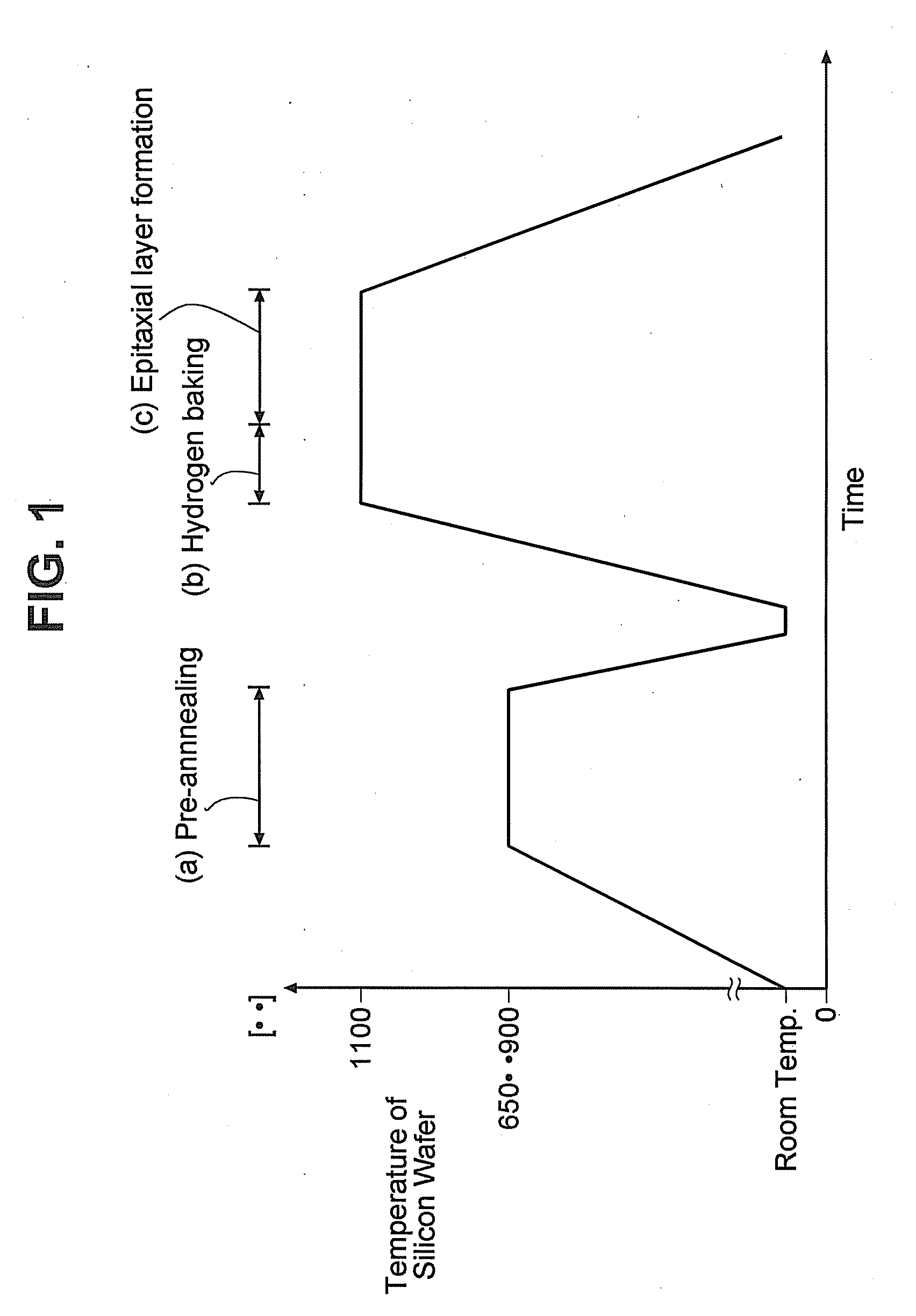
[0033]A first embodiment of the present invention will be described. As shown in FIG. 2, a method for manufacturing an epitaxial wafer of the present invention includes: a step of pulling a silicon single crystal 12 from a boron-doped silicon melt 11 in a chamber 21 based on a CZ process; and a step of forming an epitaxial layer on a surface of a silicon wafer (not shown) sliced from the silicon single crystal. In the method for manufacturing an epitaxial wafer, the silicon single crystal 12 is allowed to grow while passed through a temperature region of 800 to 600° C. in the chamber 21 in 250 minutes or less and 180 minutes or more during the pulling step. The grown silicon single crystal 12 has an oxygen concentration of 10×1017 to 12×1017 atoms / cm3 and a resistivity of 0.03 to 0.01 Ωcm. The silicon wafer is subjected to pre-annealing prior to the step of forming the epitaxial layer on the surface of the silicon wafer sliced from the silicon single crystal, for 10 minutes to 4 hou...

second embodiment

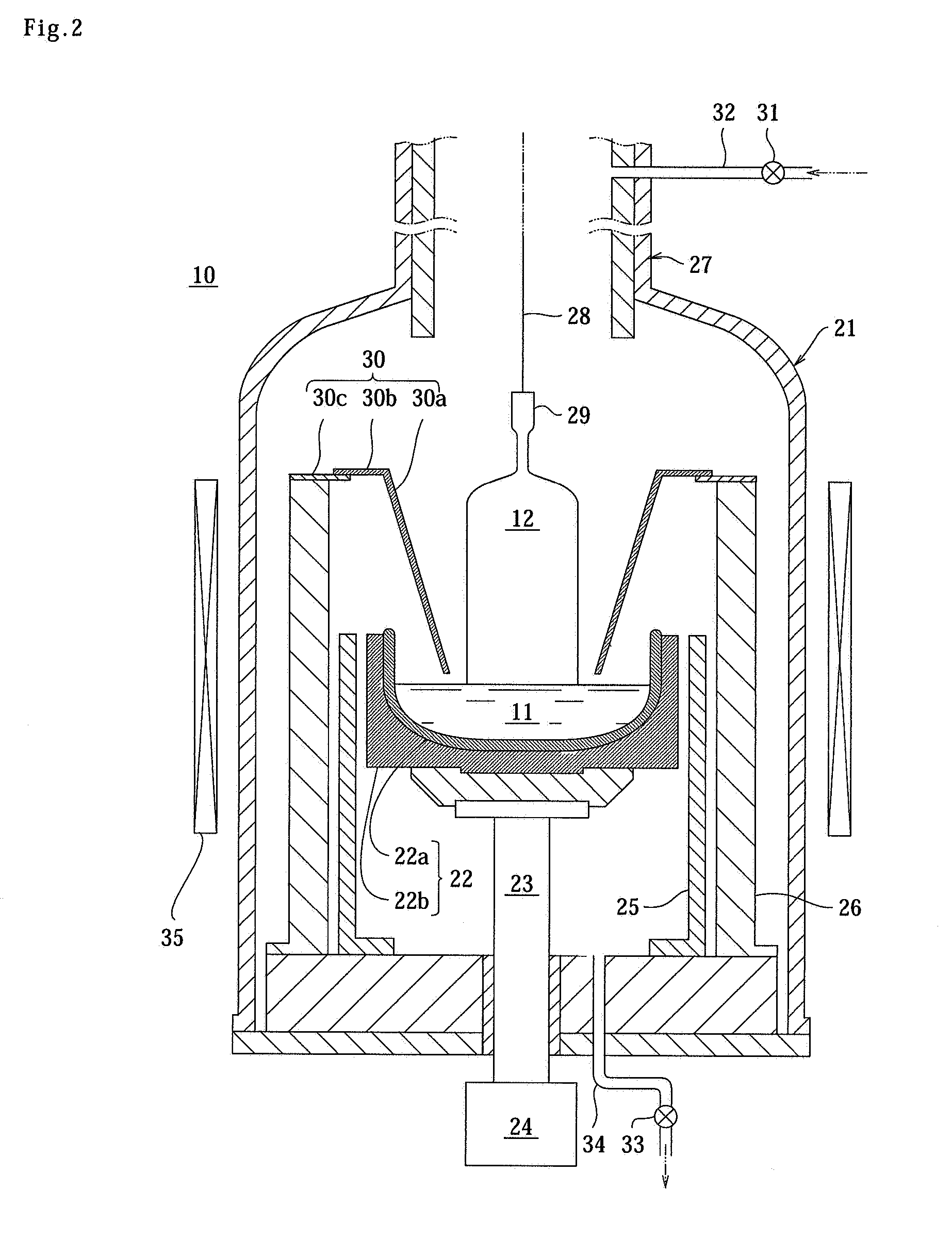
[0042]A second embodiment of the present invention will be described. A method for manufacturing an epitaxial wafer of the present invention includes: a step of pulling the silicon single crystal 12 having the diameter of 300 mm from the boron-doped silicon melt 11 in the chamber 21 through forced cooling based on a CZ process; and a step of forming an epitaxial layer on a surface of a silicon wafer sliced from the silicon single crystal. That is, in the second embodiment, as shown in FIG. 3, forced cooling is carried out with the water-cooling type cooling device 36 placed in the chamber 21. The silicon single crystal 12 is passed through a cooling cylindrical member 37 placed in the cooling device 36 and allowed to grow while passed through a temperature region of 800 to 600° C. in the chamber 21 in less than 180 minutes and 120 minutes or more during the pulling step. The grown silicon single crystal 12 has an oxygen concentration of 10×1017 to 14×1017 atoms / cm3 and a resistivity...

example 1

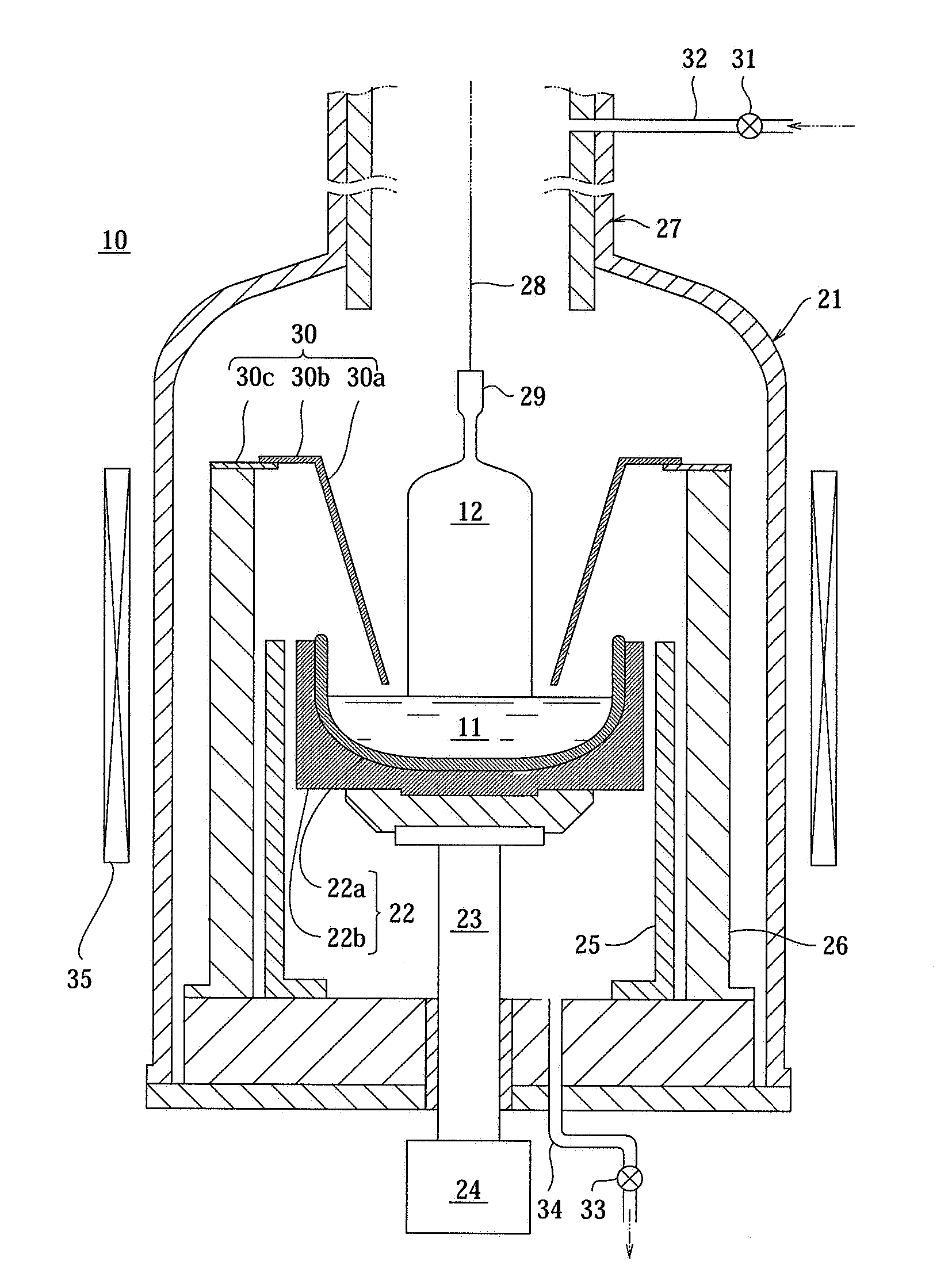
[0046]The CZ furnace 10 for growing the single crystal grows is shown in FIG. 2. To be specific, the crucible 22 for retaining the silicon melt 11 is placed at the center of the main chamber 21. The crucible 22 includes a quartz container 22a and a graphite container 22b surrounding the container 22a and is connected to a crucible driving unit 24 for rotatingly moving the crucible 22 up / down through a pivot 23. A heater 25 and a heat insulating tube 26 are concentrically arranged around the crucible 22. The silicon melt 11 prepared by melting the single crystal with the heater 25 is filled in the crucible 22.

[0047]A cylindrical pull chamber 27 is connected to the upper end of the main chamber 21, and a seed pulling unit (not shown) is provided at the upper end of the pull chamber 27. A wire cable 28, from which a seed crystal 29 is suspended, is set in a rotatable and vertically movable state. The silicon single crystal 12 can be allowed to grow from the lower end of the seed crysta...


PUM

PropertyMeasurementUnit
temperatureaaaaaaaaaa
resistivityaaaaaaaaaa
temperatureaaaaaaaaaa

Abstract

A method for manufacturing an epitaxial wafer includes: a step of pulling a single crystal from a boron-doped silicon melt in a chamber based on a Czochralski process; and a step of forming an epitaxial layer on a surface of a silicon wafer sliced from the single crystal. The single crystal is allowed to grow while passed through a temperature region of 800 to 600° C. in the chamber in 250 to 180 minutes during the pulling step. The grown single crystal has an oxygen concentration of 10×1017 to 12×1017 atoms / cm3 and a resistivity of 0.03 to 0.01 Ωcm. The silicon wafer is subjected to pre-annealing prior to the step of forming the epitaxial layer on the surface of the silicon wafer, for 10 minutes to 4 hours at a predetermined temperature within a temperature region of 650 to 900° C. in an inert gas atmosphere. The method is to fabricate an epitaxial wafer that has a diameter of 300 mm or more, and that attains a high IG effect, and involves few epitaxial defects.

Description

BACKGROUND OF THE INVENTION[0001]1. Field of the Invention[0002]The present invention relates to improvements in a method for manufacturing an epitaxial wafer used for a highly integrated semiconductor device, and, more particularly to a method for manufacturing an epitaxial wafer, which aims at forming an epitaxial layer on a silicon wafer sliced from silicon single crystal that grows based on a Czochralski process (hereinafter referred to as “CZ process”).[0003]2. Description of the Related Art[0004]Hitherto, an epitaxial wafer used as a substrate of a highly integrated device has been fabricated by forming an epitaxial layer on a silicon wafer sliced from a silicon single crystal that grows based on a Czochralski process (hereinafter referred to as “CZ process”).[0005]The CZ process is a method of melting polysilicon filled in a crucible under heating with a heater and then dipping seed crystal into a surface portion of the silicon melt to rotate and allow the crystal to grow, an...

Claims


Application Information

Patent Timeline
Patent Type & Authority Applications(United States)
IPC IPC(8): C30B15/00B32B3/00H01L21/20
CPCC30B15/206C30B25/20Y10T428/26C30B33/02H01L21/3225C30B29/06H01L21/20
Inventor KOIKE, YASUOONO, TOSHIAKIIKEDA, NAOKIKATANO, TOMOKAZU
Owner SUMCO CORP
Why Eureka
Try Eureka