Semiconductor device, leadframe and structure for mounting semiconductor device

a semiconductor device and leadframe technology, applied in semiconductor devices, semiconductor/solid-state device details, electrical apparatus casings/cabinets/drawers, etc., can solve the problems of lead formation and interference, stage bars (support bars) cannot support the die stage, and the fabrication of semiconductor devices becomes complicated

Inactive Publication Date: 2008-11-27
FUJITSU MICROELECTRONICS LTD
View PDF7 Cites 9 Cited by
  • Summary
  • Abstract
  • Description
  • Claims
  • Application Information

AI Technical Summary

Benefits of technology

[0025]An object of the present invention is to provide a structure of a semiconductor device, in which intervals are enabled to be narrowed between leads arranged around a semiconductor element to increase the number of leads, and electrical interference is prevented or reduced between the leads so that no crosstalk occurs between the leads.

Problems solved by technology

However, narrowing intervals between the leads 73 causes difficult lead formation as well as interference therebetween when the semiconductor device is in operation.
This results in crosstalk.
However, the extended die stage bars (support bars) cannot support the die stage in this case.
Thus, the semiconductor device fabrication becomes complicated, and the signal leads cannot be shielded sufficiently.

Method used


Image

  • Semiconductor device, leadframe and structure for mounting semiconductor device
  • Semiconductor device, leadframe and structure for mounting semiconductor device
  • Semiconductor device, leadframe and structure for mounting semiconductor device

Examples


example 1

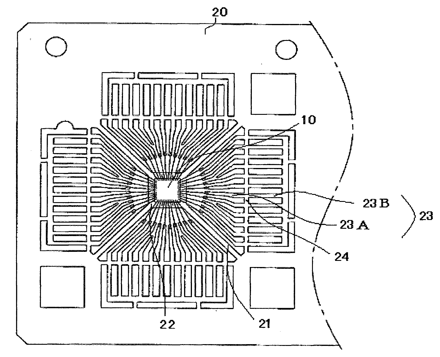
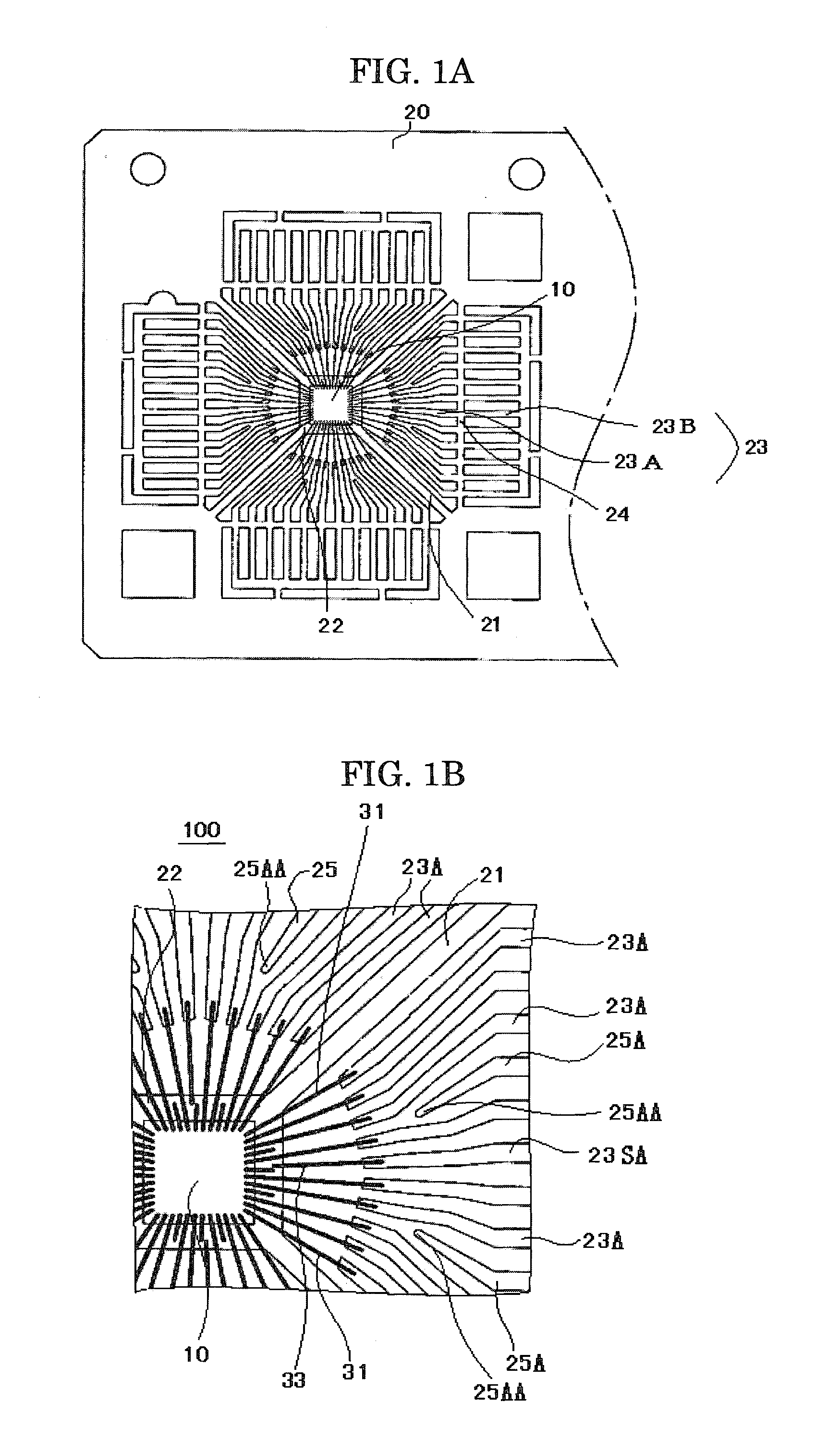
[0044]A semiconductor device 100, a first example of the semiconductor device according to the present invention, is described with reference to FIGS. 1A, 1B and 2.

[0045]FIG. 1A shows a leadframe of the semiconductor device 100 and an arrangement of a semiconductor element mounted on the leadframe. FIG. 1B shows an enlarged essential part of FIG. 1A.

[0046]In this example, a semiconductor element 10 is mounted on and adhered to a rectangular die stage 22 of a leadframe 20, and die stage bars 21 support four corners of the die stage 22. Electrode terminals of the semiconductor element 10 are connected to leads 23 of the leadframe 20 through bonding wires 31 and optionally to the die stage 22.

[0047]The plurality of leads 23 (first leads) are aligned on substantially the same plane around the die stage 22. Each lead 23 has sections called an inner lead 23A and an outer lead 23B through a tie bar (dambar) 24. The inner lead 23A is closer to the die stage 22 (inner side) than the outer le...

example 2

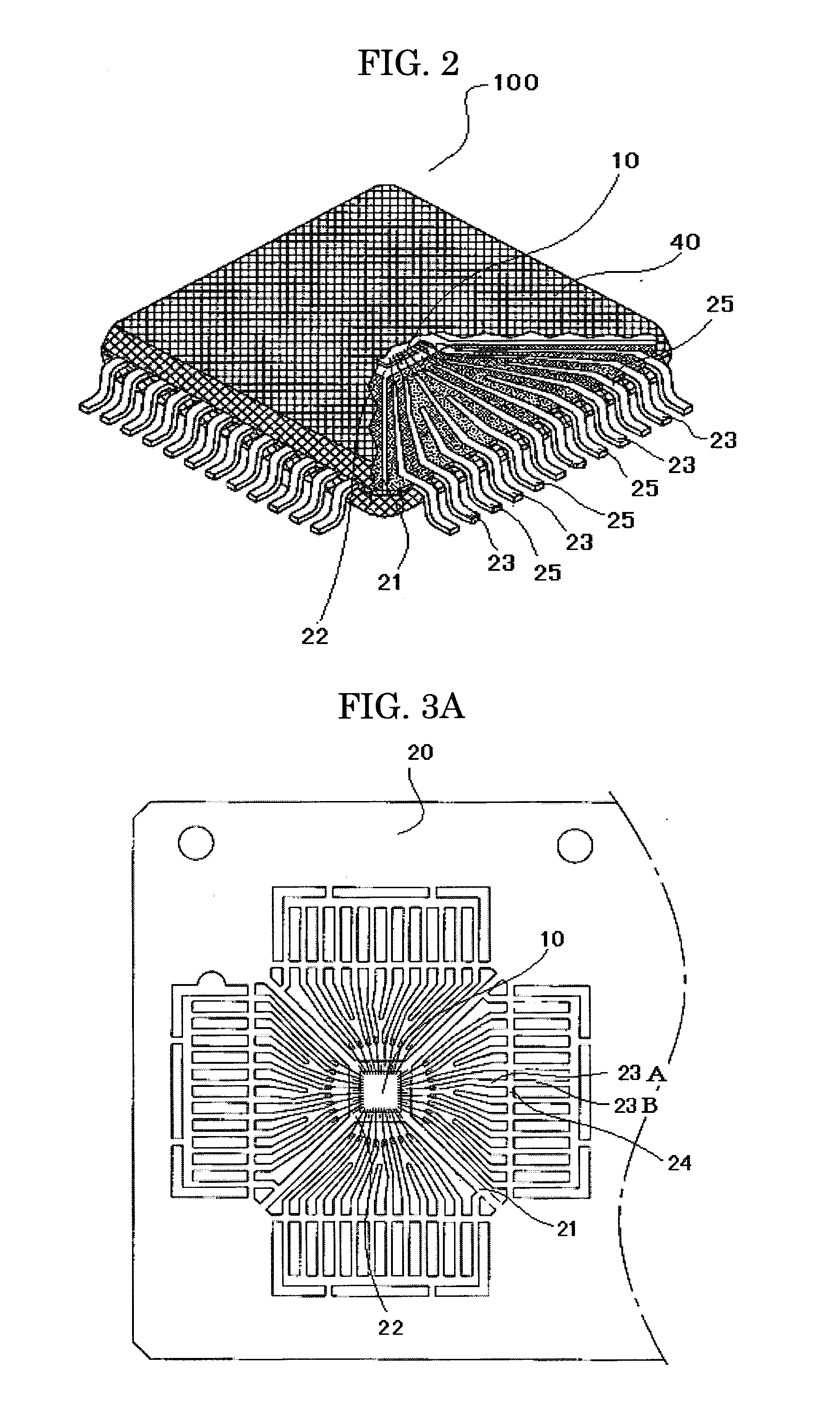
[0071]A semiconductor device 200, a second example of the semiconductor device according to the present invention, is described with reference to FIGS. 3A and 3B.

[0072]FIG. 3A shows a leadframe of the semiconductor device 200 and an arrangement of a semiconductor element mounted on the leadframe. FIG. 3B shows an enlarged essential part of FIG. 3A.

[0073]Note that the same reference numerals are used for components corresponding to those of the semiconductor device 100 shown in FIGS. 1A, 1B and 2.

[0074]Similar to the first example, a semiconductor element 10 is mounted on and adhered to a rectangular die stage 22 of a lead frame 20, and die stage bars 21 support four corners of the die stage 22. Electrode terminals of the semiconductor element 10 are connected to leads 23 of the leadframe 20 through bonding wires 31 and optionally to the die stage 22.

[0075]The plurality of leads 23 (first leads) are aligned on substantially the same plane around the die stage 22. Each lead 23 has sec...

example 3

[0082]A semiconductor device 300, a third example of the semiconductor device according to the present invention, is described with reference to FIGS. 4A and 4B.

[0083]FIG. 4A shows a leadframe of the semiconductor device 300 and an arrangement of a semiconductor element mounted on the leadframe. FIG. 4B shows an enlarged essential part of FIG. 4A.

[0084]Note that the same reference numerals are used for components corresponding to those of the semiconductor devices 100 or 200 shown in FIGS. 1A, 1B, 2, 3A and 3B.

[0085]Similar to the first and second examples, a semiconductor element 10 is mounted on and adhered to a rectangular die stage 22 of a leadframe 20, and die stage bars 21 support four corners of the die stage 22. Electrode terminals of the semiconductor element 10 are connected to leads 23 of the leadframe 20 through bonding wires 31 and optionally to the die stage 22.

[0086]The plurality of leads 23 (first leads) are aligned on substantially the same plane around the die stag...


PUM


Abstract

A structure of a semiconductor device is provided, where intervals can be narrowed between leads arranged around a semiconductor element to increase the number of leads, and electrical interference is prevented or reduced between the leads to cause no crosstalk between the leads. The semiconductor device of the present invention includes a semiconductor element and a plurality of leads arranged around the semiconductor element. The plurality of leads include a plurality of first leads and a plurality of second leads. The plurality of first leads are connected to electrode terminals of the semiconductor element through connection members. The plurality of second leads are arranged between the first leads and are not connected to the electrode terminals of the semiconductor element.

Description

CROSS-REFERENCE TO RELATED APPLICATIONS[0001]This application is based upon and claims the benefits of the priority from the prior Japanese Patent Application No. 2007-138984 filed on May 25, 2007, the entire contents of which are incorporated herein by reference.BACKGROUND OF THE INVENTION[0002]1. Field of the Invention[0003]The present invention relates to a semiconductor device, a leadframe and a structure for mounting the semiconductor device and, more particularly, to a semiconductor device, a leadframe and a structure for mounting the semiconductor device, which ease fine pitch inner leads arrangement to increase the number of pins.[0004]2. Description of the Related Art[0005]As the performance of electronic equipment is improved with size reduction, fast and high performance semiconductor devices (e.g., a semiconductor integrated circuit device installed in the electronic equipment) are demanded with further size and weight reductions.[0006]For example, external connection te...

Claims


Application Information

Patent Timeline
Patent Type & Authority Applications(United States)
IPC IPC(8): H01L23/495H05K7/18
CPCH01L23/49541H01L23/552H01L24/45H01L24/49H01L24/85H01L2224/45124H01L2224/45144H01L2224/45147H01L2224/48091H01L2224/48247H01L2224/48257H01L2224/49171H01L2224/49433H01L2224/85439H01L2924/01004H01L2924/01005H01L2924/01013H01L2924/01014H01L2924/01028H01L2924/01029H01L2924/01031H01L2924/01033H01L2924/01047H01L2924/01075H01L2924/01078H01L2924/01079H01L2924/01082H01L2924/09701H01L2924/10329H01L2924/14H01L2924/19043H01L2924/19107H01L2924/3025H01L2924/00014H01L24/48H01L2924/01006H01L2924/014H01L2924/00H01L2924/00012H01L2224/48639H01L2224/48839H01L2224/48739H01L2924/181H01L23/48
Inventor YURINO, TAKAHIRO
Owner FUJITSU MICROELECTRONICS LTD
Why Eureka
Try Eureka