Source biasing of nor-type flash array with dynamically variable source resistance

a source resistance and flash array technology, applied in the direction of digital storage, instruments, semiconductor devices, etc., can solve the problems of over-erasure, biasing the commonly connected source regions of such devices, and affecting the speed at which large amounts of new data can be written into flash memory chips, etc., to achieve the effect of limiting the speed at which large amounts of new data can be written

Inactive Publication Date: 2008-11-27
PROMOS TECH PTE LTD
View PDF7 Cites 17 Cited by
  • Summary
  • Abstract
  • Description
  • Claims
  • Application Information

AI Technical Summary

Benefits of technology

[0006]During the soft-programming (Vt compaction) process, voltages will be applied to one over-erased transistor for repairing it by shifting its programmable Vt slightly higher. However, adjacent and still not-yet-repaired transistors (of the same sector) may continue to leak large amounts leakage current by way of the same or other bit lines. This leakage current pulls down an output voltage of an on-chip charge pump and interferes with the circuit's ability to soft-program more than one over-erased transistor at a time. In turn, the inability to soft-program many transistors at once limits the number of transistors that can be placed in a flash-erasable sector and thus limits the speed at which large amounts of new data can be written into a flash memory chip.

Problems solved by technology

So is the problem of biasing the commonly connected source regions of such devices.
When large blocks or sectors of floating gate transistors are flash erased, an associated problem known as over-erasure often occurs.
Such abnormally low or negative Vt's make it difficult to stop current from leaking through the over-erased transistors even though a turn-off voltage such as VGoff=0V is applied.
However, adjacent and still not-yet-repaired transistors (of the same sector) may continue to leak large amounts leakage current by way of the same or other bit lines.
This leakage current pulls down an output voltage of an on-chip charge pump and interferes with the circuit's ability to soft-program more than one over-erased transistor at a time.
In turn, the inability to soft-program many transistors at once limits the number of transistors that can be placed in a flash-erasable sector and thus limits the speed at which large amounts of new data can be written into a flash memory chip.
Light doping of transistor sources is not without its drawbacks however.
Practitioners are therefore caught in a Hobson's choice dilemma between having to accept large leakage currents during soft programming if they don't employ light source doping or having to accept reduced read currents if they do employ light source doping.
Reduction of read currents causes the memory to be more susceptible to noise problems.

Method used


Image

  • Source biasing of nor-type flash array with dynamically variable source resistance
  • Source biasing of nor-type flash array with dynamically variable source resistance
  • Source biasing of nor-type flash array with dynamically variable source resistance

Examples


Embodiment Construction

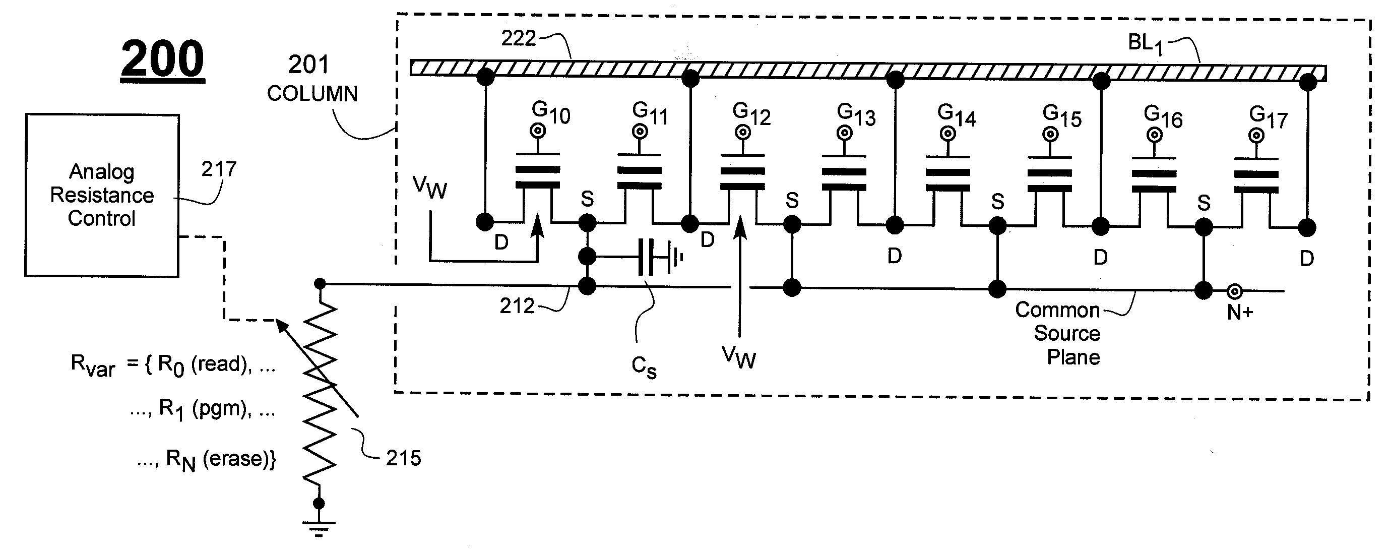
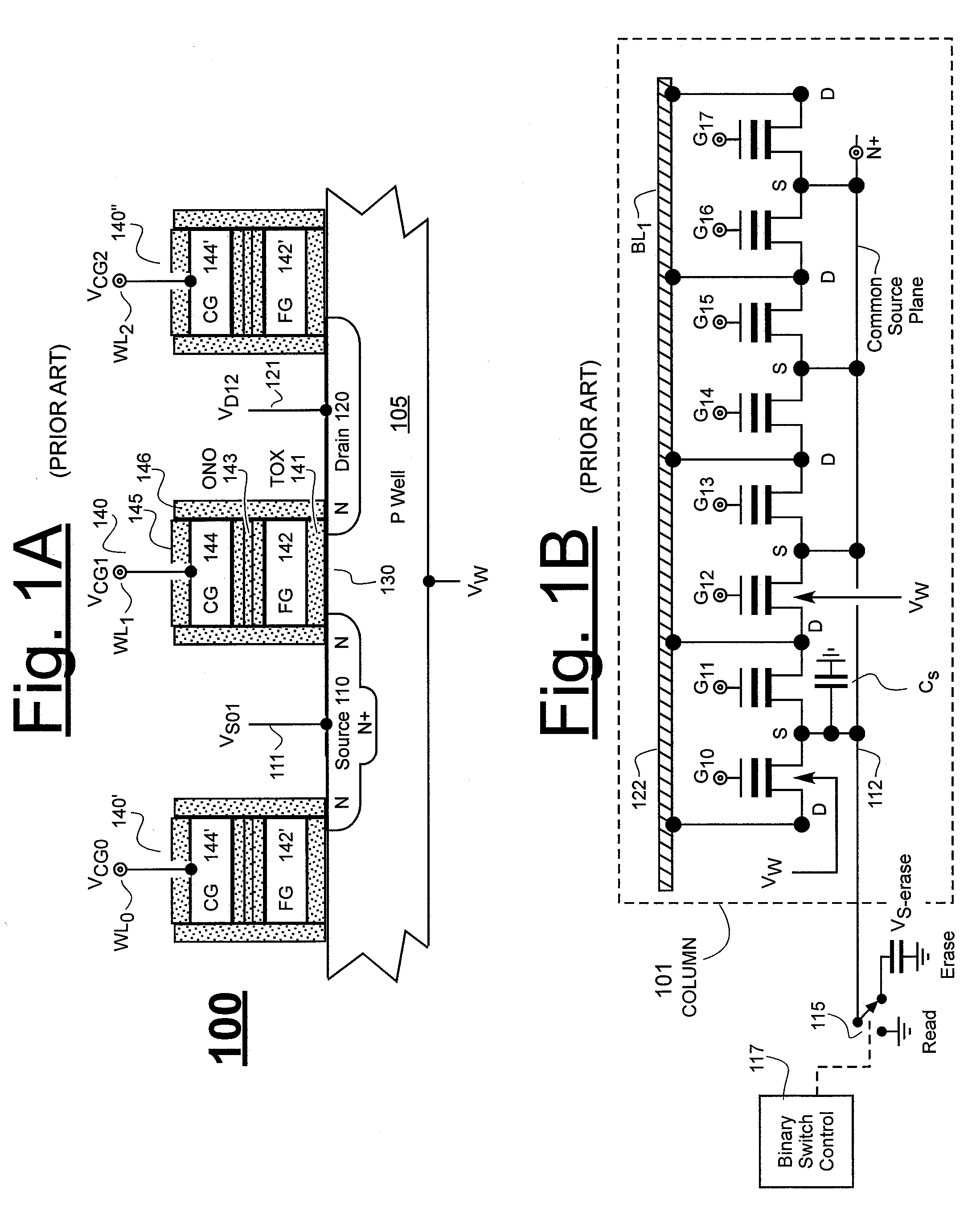
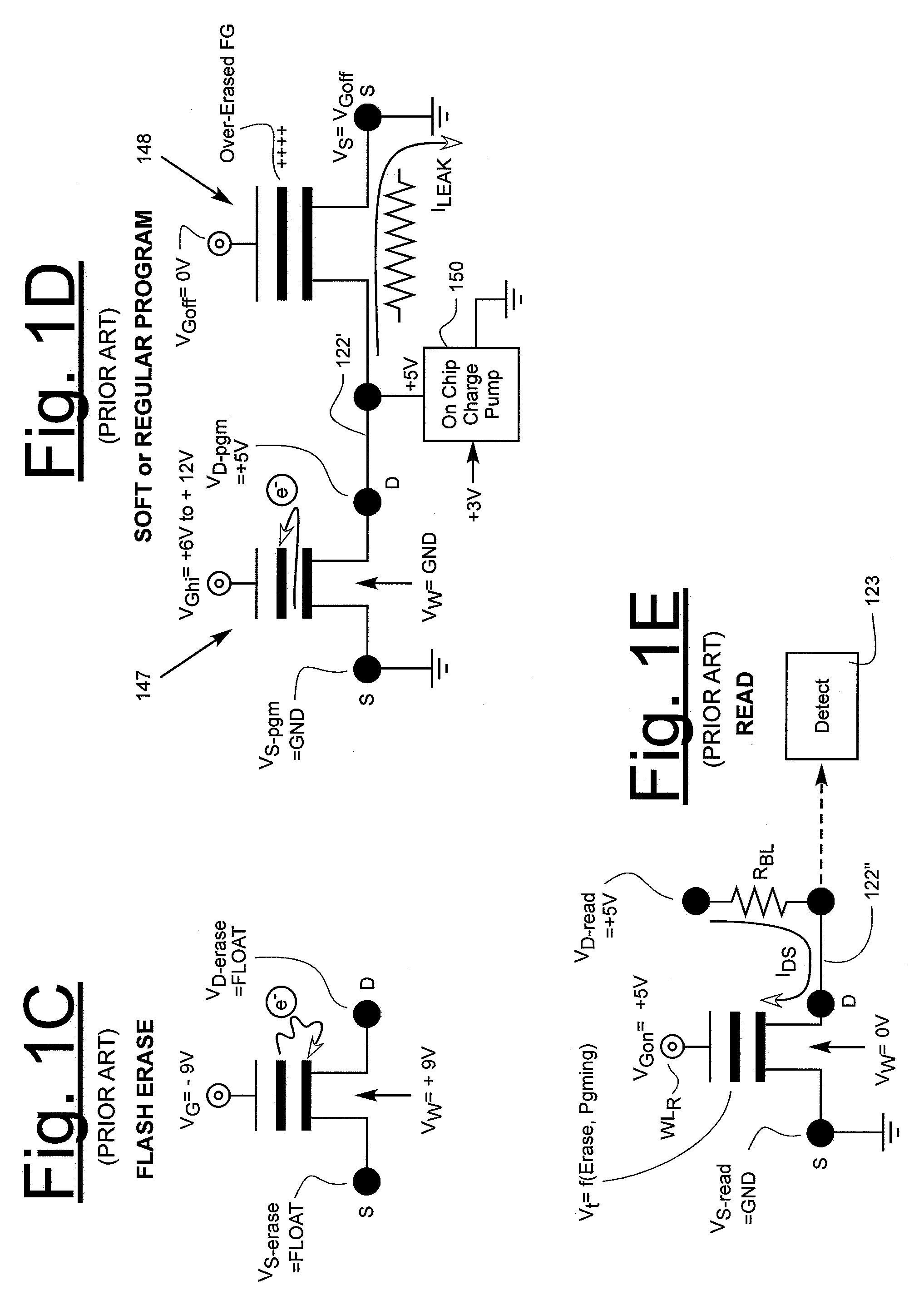
[0024]FIG. 1A is a schematic cross sectional side view showing three floating gate transistors in a NOR-array column of a conventional Flash memory device 100. The central gate stack 140 (coupled to word line WL1) defines part of a first nonvolatile memory cell that includes an N-type source region 110, an N-type drain region 120, and a P-type channel region 130. The source and drain regions, 110 and 120, are implanted in a P-well 105 that is contiguous with the channel region 130. The source, drain, channel and well regions may be integrally formed in a monolithic semiconductor substrate (i.e., monocrystalline silicon) by way of various well known doping techniques such as ion implant.

[0025]Source region 110 is in communication with a common source line (112 of FIG. 1B) by way of a source contact 111, while drain region 120 is in communication with a column bit line (122 of FIG. 1B) by way of a drain contact 121. Source contact 111 and drain contact 121 may be separated from the st...


PUM


Abstract

A dynamically variable source resistance is provided for each sector of a NOR-type Flash memory device. The variable source resistance of a given sector is set to a relatively low value (i.e., close to zero) during read operations. The variable source resistance is set to a relatively high impedance value (i.e., close to being an open circuit) during flash erase operations. The variable source resistance is set to a first intermediate resistance value at least during soft-programming where the first intermediate resistance value is one that raises VS and thus drives VGS below local threshold even for over-erased transistors of the sector that have a VGoff de-assertion voltage applied to their control gates for purpose of turning those transistors off. In one embodiment, the variable source resistance is set to a second intermediate resistance value during a testing mode that tests the extent to which the corresponding sector has been over-erased. The results of the testing mode are then used to intelligently optimize the number of transistors that are simultaneously soft-programmed in that sector during each Vt compaction cycle.

Description

FIELD OF DISCLOSURE[0001]The present disclosure of invention relates generally to NOR-type Flash memory arrays and more specifically to methods of biasing the commonly connected source regions of each sector of a NOR-type Flash memory during read, write (program), and erase (blanket clear) operations.DESCRIPTION OF RELATED ART[0002]NOR-type Flash memory arrays are well known. So is the problem of biasing the commonly connected source regions of such devices. Examples of patents that deal with the problem include: U.S. Pat. No. 6,570,787 (Wang et al 2003) and U.S. Pat. No. 6,852,594 (Wang et al 2005).[0003]Briefly, NOR-type Flash memory arrays are referred to as such because pairs of adjacent floating gate transistors share a common source region in order to provide a compact layout. Typically, each floating gate transistor comprises a source region, a drain region, a channel region (disposed between the source and drain and also disposed above a substrate well), a tunnel insulator l...

Claims


Application Information

Patent Timeline
Patent Type & Authority Applications(United States)
IPC IPC(8): G11C11/34H01L29/788
CPCG11C16/3404G11C16/3409
Inventor WANG, DANIEL C.HE, YUE-SONG
Owner PROMOS TECH PTE LTD
Why Eureka
Try Eureka