Sintered power semiconductor substrate and method of producing the substrate

a technology of semiconductor substrate and substrate, which is applied in the direction of solid-state devices, synthetic resin layered products, metal-layer products, etc., can solve the problems of substrate being bowed, and achieve the effect of simple production method, low cost and little bowing

Inactive Publication Date: 2008-11-27
SEMIKRON ELECTRONICS GMBH & CO KG
View PDF21 Cites 5 Cited by
  • Summary
  • Abstract
  • Description
  • Claims
  • Application Information

AI Technical Summary

Benefits of technology

[0008]It is an object of the invention to provide a power semiconductor substrate with little bowing and a simple, low-cost method of producing such a power semiconductor substrate.
[0018]It may be preferred if the pasty layer is applied by means of screen printing. In this fashion, the necessary positioning accuracy can be achieved along with the required layer thickness, all at relatively low cost.

Problems solved by technology

A disadvantage of such DCB substrates is that, due to the exposure to high temperature during the production process, immediately after the production process or in a later process step, for example during the buildup of a power semiconductor module, the substrate may become bowed.

Method used


Image

  • Sintered power semiconductor substrate and method of producing the substrate
  • Sintered power semiconductor substrate and method of producing the substrate

Examples


Embodiment Construction

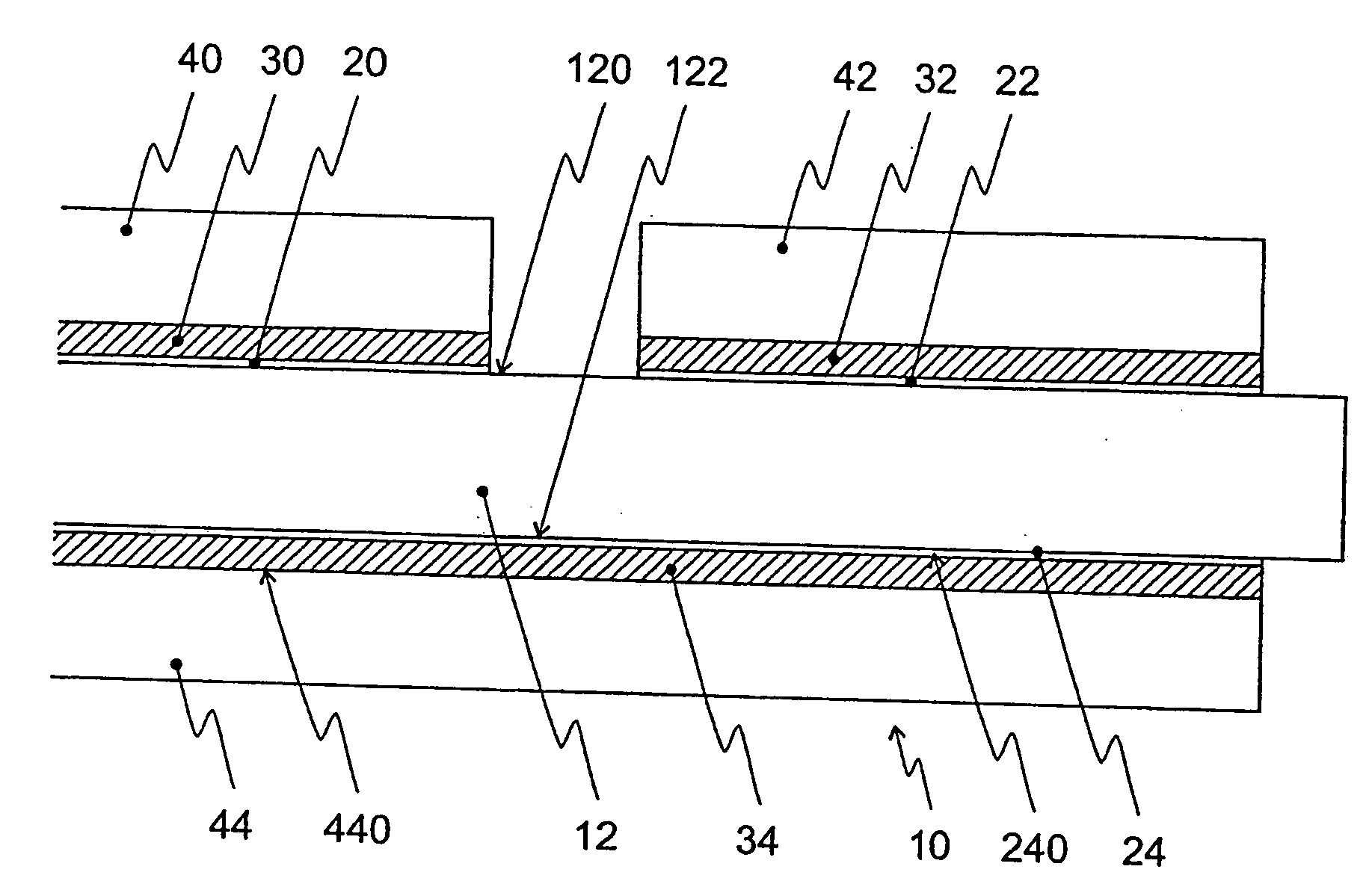
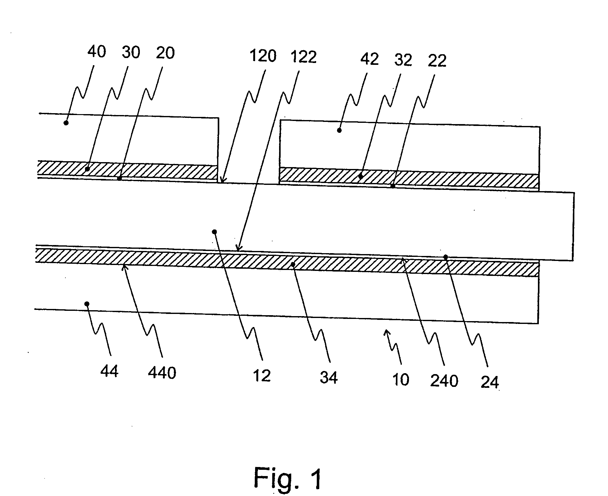
[0022]Particularly preferred developments of this power semiconductor substrate and of the production process are described with reference to the exemplary embodiment illustrated in the FIGURE.

[0023]The FIGURE shows a power semiconductor substrate 10 according to the invention. The power semiconductor substrate 10 has an insulating base 12 having a sheet-like form. Base 12 should have a high electrical resistance with a low thermal resistance, for which reason an industrial ceramic, such as for example aluminium oxide, aluminium nitrite or silicon nitrite, is particularly suitable. A particularly good compromise of these requirements with low-cost production is offered by aluminium oxide.

[0024]In preparation for the following sintered connection, a thin film of an adhesion promoting layer 20, 22, 24 is applied to both main areas 120, 122 of base 12, preferably over its full surface area, the production process for this layer not being the subject of this invention. The adhesion prom...


PUM

PropertyMeasurementUnit
thicknessaaaaaaaaaa
thicknessaaaaaaaaaa
thicknessaaaaaaaaaa

Abstract

A power semiconductor substrate with an insulating sheet-like base, having at least one sequence of layers of: a thin adhesion promoting layer, a sintered metal layer and a conductive layer arranged on at least one main area of the substrate. The associated process includes the steps of: coating at least a portion of the one main area with the adhesion promoting layer; arranging a pasty layer of the sintered metal and a solvent on at least a portion of the adhesion promoting layer; arranging the conductive layer on the sintered metal layer; and applying pressure to the conductive layer of the power substrate.

Description

BACKGROUND OF THE INVENTION[0001]1. Field of the Invention[0002]The invention is directed to a power semiconductor substrate with an insulating base and at least one conductor track and a method for producing such a substrate.[0003]2. Description of the Related Art[0004]Such power semiconductor substrates have so far been known for example in the form of AMB (active metal braze), DCB (direct copper bonding) or IMS (insulated metal substrate) substrates.[0005]The at least one conductor track provides electrically conductive connection, for example, to power semiconductor devices or to internal and / or external connecting elements. Such connecting elements may be formed with the conductor track for example by means of soldering or brazing connections, or by means of pressure-contacted connections.[0006]According to the prior art, there are known DCB substrates that comprise a ceramic base body, often aluminium oxide or aluminium nitride, with conductor tracks of a copper foil arranged ...

Claims


Application Information

Patent Timeline
Patent Type & Authority Applications(United States)
IPC IPC(8): B32B18/00B32B5/00B32B38/14
CPCH01L23/3735H05K1/0306Y10T428/264H05K2201/0355H01L2224/75315H05K3/38C04B35/645C04B37/026C04B2237/125C04B2237/408C04B2237/706C04B37/021C04B2237/124C04B2237/343C04B2237/366C04B2237/368C04B2237/407C04B2237/704C04B2237/72Y10T428/31678H01L21/4867
Inventor GOBL, CHRISTIANBRAML, HEIKOHERMANN, ULRICH
Owner SEMIKRON ELECTRONICS GMBH & CO KG
Why Eureka
Try Eureka