Conductive nitride semiconductor substrate and method for producing the same

a technology of conductive nitride and semiconductor substrate, which is applied in the direction of single crystal growth, polycrystalline material growth, chemistry apparatus and processes, etc., can solve the problems of inability to form to a thickness of 70 m or more, inapplicability of /sub>gacl of 1 kpa, and inability to achieve partial formation of gacl, etc., to achieve complementarity and uniformity reduce dislocation density density ratio

Inactive Publication Date: 2012-02-07
SUMITOMO ELECTRIC IND LTD
View PDF19 Cites 12 Cited by
  • Summary
  • Abstract
  • Description
  • Claims
  • Application Information

AI Technical Summary

Benefits of technology

[0101]ELO cannot sufficiently reduce dislocations. Facet growth, proposed in Patent Documents 8 and 9, have the effect of reducing dislocation density. Currently known methods for forming conductive GaN include oxygen doping and silicon doping. For oxygen doping, as in Patent Documents 6 and 7, water or oxygen may be mixed in a source gas. These are safe substances. For silicon doping, as in Patent Documents 4 and 5, silane (SiH4) gas must be supplied. Silane gas is a hazardous gas and therefore should not be used in large quantities. In addition, it is uncertain whether or not the absorption of SiH4 gas has plane dependence. There is no research as to whether or not silicon doping has anisotropy for the c-plane and the m- or a-plane, or generally a facet plane (hereinafter abbreviated to “f-plane”). If silicon has the same plane orientation dependence as oxygen, the dosage of the n-type impurity cannot be made uniform. However, if silicon and oxygen have different plane dependence, the resistivity may be complementarily made uniform.
[0102]Facet growth is effective in reducing dislocation density. By causing dislocations to cluster into closed defect cluster regions above the masking portions, the dislocation density can be reduced in other portions. In addition, the substrate has little bow and low cracking ratio because it has a rough surface.

Problems solved by technology

Patent Document 2 discloses that a crystal formed at a GaCl partial pressure PGaCl of 1 kPa is impractical because it has a flat surface but has large bow and large internal stress and cracks easily, and it cannot be formed to a thickness of 70 μm or more.
However, it is unknown what level oxygen forms in GaN, and it is therefore uncertain whether oxygen serves as an n-type dopant unless a doping test is carried out in practice.
The use of a large amount of silane gas for growth of an n-type substrate is hazardous because it has the risk of explosion.
Patent Document 6, however, only first pointed out that oxygen can serve as an n-type dopant and does not recognize anisotropy in doping.
The resultant crystal has noticeable surface irregularities.
Because the pit positions are randomly determined, it is difficult to fabricate devices on the substrate.
In Patent Document 9, because the mask has a regularly distributed isolated dot pattern, the closed defect cluster regions H are formed above the dots (masking portions), and the single-crystal low-dislocation-density concomitant regions Z and the single-crystal low-dislocation-density remaining region Y are formed therearound above the exposed portion E. The dispersed closed defect cluster regions H are disadvantageous in fabricating devices such as semiconductor lasers or light-emitting diodes on the substrate.
For light-emitting devices, dislocations may lead to deterioration because a high-density current flows through the substrate.
However, there are other problems.
A substrate having high dislocation density is undesirable because it causes current leakage.
ELO cannot sufficiently reduce dislocations.
In addition, it is uncertain whether or not the absorption of SiH4 gas has plane dependence.
If silicon has the same plane orientation dependence as oxygen, the dosage of the n-type impurity cannot be made uniform.
One of the disadvantages is anisotropy in oxygen absorption during oxygen doping.

Method used


Image

  • Conductive nitride semiconductor substrate and method for producing the same
  • Conductive nitride semiconductor substrate and method for producing the same
  • Conductive nitride semiconductor substrate and method for producing the same

Examples


examples

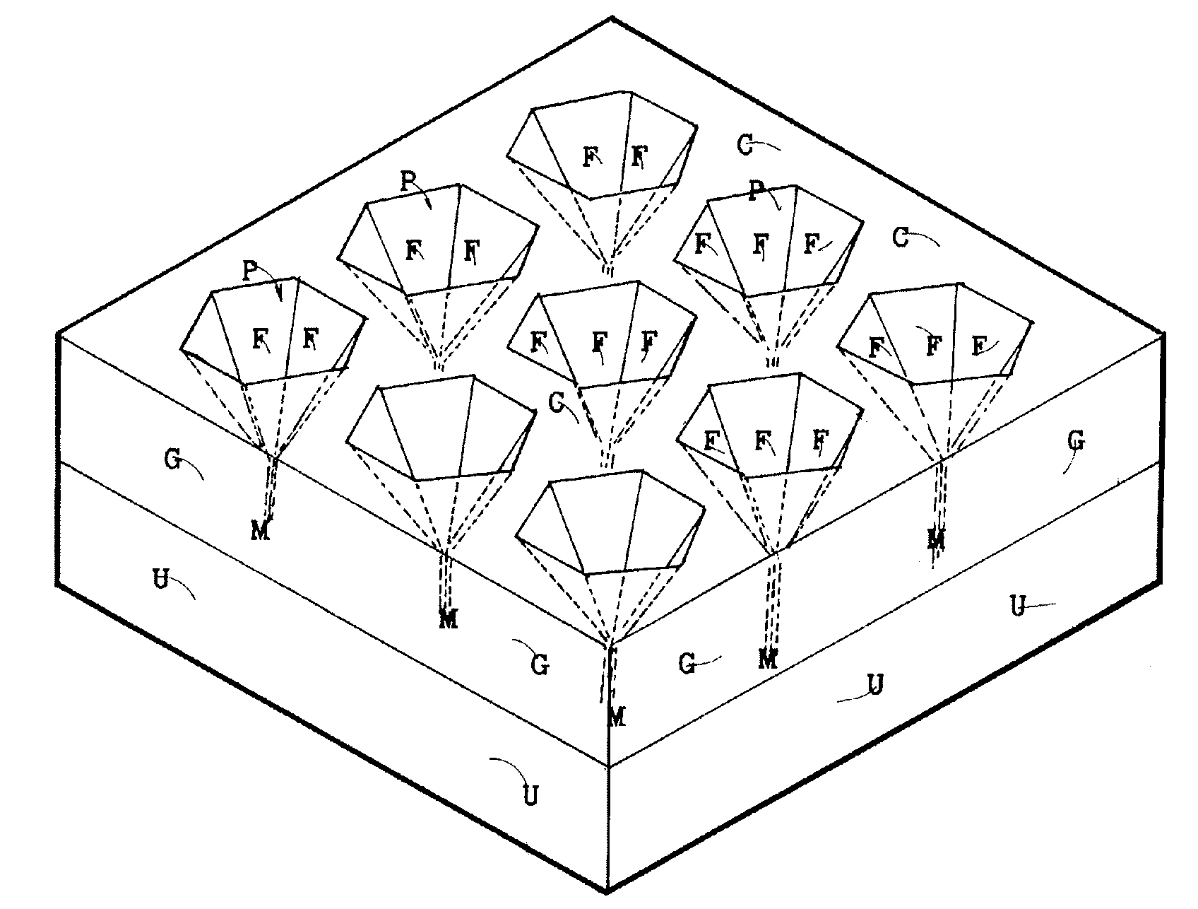
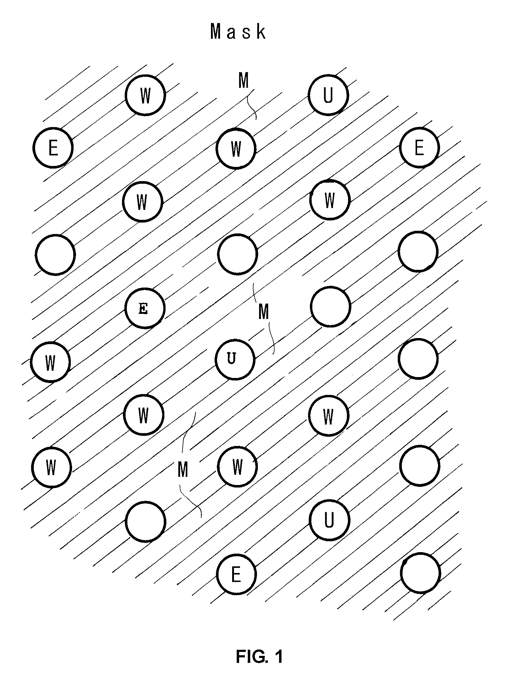
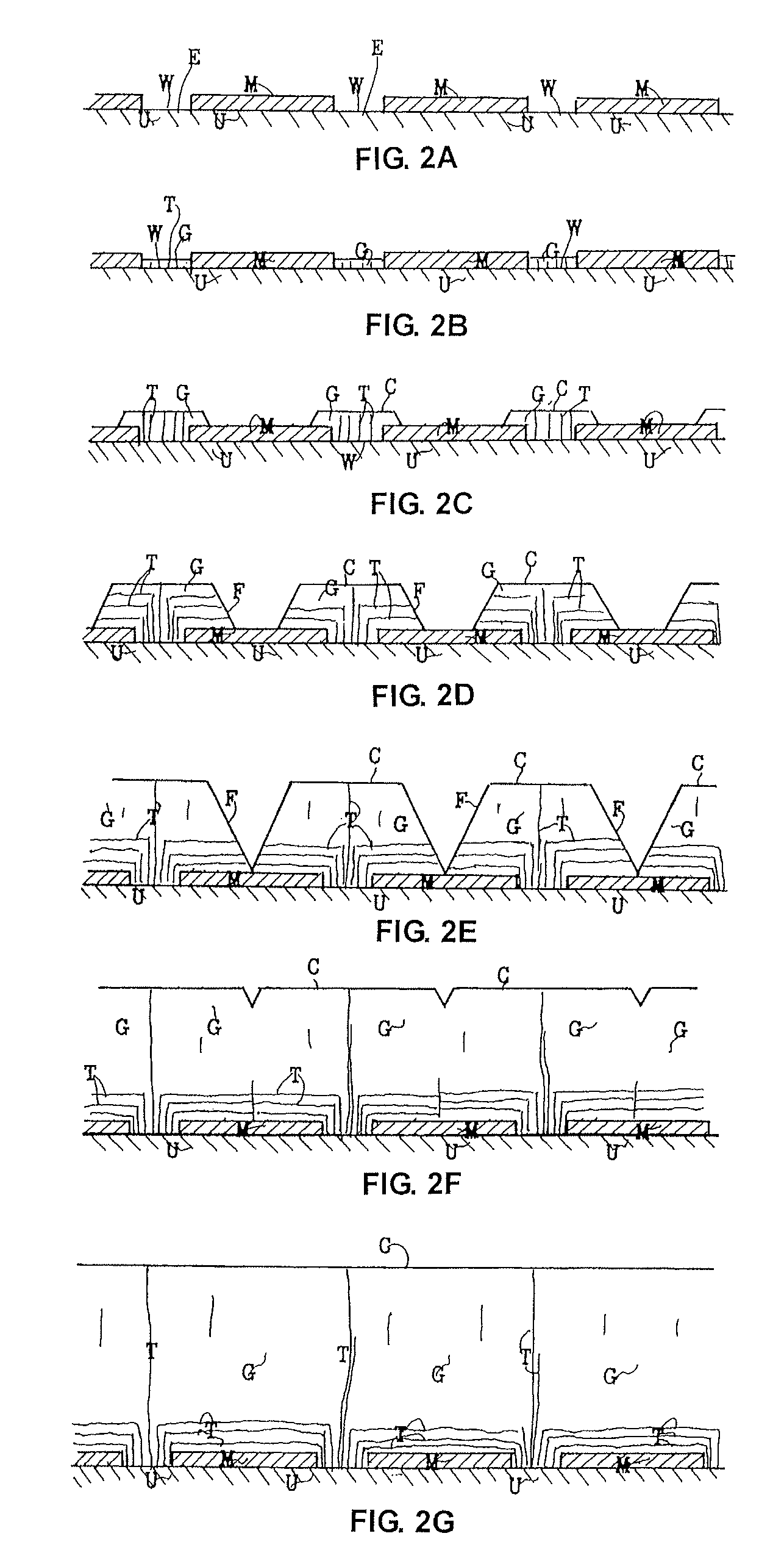
[0205]Dot masks or stripe masks were formed on GaAs substrates having (111) Ga-plane serving as underlying substrates. The masks were formed of SiO2 and had a thickness of 60 to 200 nm. The ranges of dimensions (s, w, and p) of the masks were 10 μm≦s≦100 μm and 250 μm≦w≦10,000 μm. The dimensions and shapes of the masks of the individual samples will be described later. A GaN film was then grown on the substrates by HVPE. Specifically, a buffer layer was initially formed, and a thick epitaxial layer was then formed thereon. A total of 45 different types of samples were prepared. The growth conditions for the buffer layer were as follows:

[0206]Substrate temperature: 500° C. to 550° C.

[0207]GaCl partial pressure PGaCl: 80 Pa (0.0008 atm)

[0208]NH3 partial pressure PNH3: 16 kPa (0.16 atm)

[0209]Thickness of buffer layer: 50 nm

[0210]The buffer layer was grown at a V / III ratio b of 200. Although the growth temperature and the V / III ratio b are important in the present invention, they are im...


PUM

PropertyMeasurementUnit
diameteraaaaaaaaaa
diameteraaaaaaaaaa
resistivityaaaaaaaaaa

Abstract

A method for producing a conductive nitride semiconductor substrate circuit includes the steps of forming, on an underlying substrate, a mask including dot or stripe masking portions having a width or diameter of 10 to 100 μm and arranged at a spacing of 250 to 10,000 μm; growing a nitride semiconductor crystal on the underlying substrate by hydride vapor phase epitaxy (HVPE) at a growth temperature of 1,040° C. to 1,150° C. by supplying a group III source gas, a group V source gas, and a silicon-containing gas in a V/III ratio of 1 to 10; and removing the underlying substrate, thus forming a free-standing conductive nitride semiconductor crystal substrate having a resistivity r of 0.0015 Ωcm≦r≦0.01 Ωcm, a thickness of 100 μm or more, and a radius of bow curvature U of 3.5 m≦U≦8 m.

Description

BACKGROUND OF THE INVENTION[0001]1. Field of the Invention[0002]The present invention relates to conductive nitride semiconductor substrates and methods for producing such substrates. Nitride semiconductors include gallium nitride (GaN), aluminum nitride (AlN), indium nitride (InN), and mixed crystals such as InGaN and AlInGaN. The invention is directed not to thin films deposited on underlying substrates, but to free-standing crystal substrates. Here, GaN will be mainly discussed. GaN, which has a wide bandgap, is used as a material for blue light-emitting devices.[0003]In the related art, blue light-emitting devices such as light-emitting diodes and semiconductor lasers are produced by epitaxially growing a nitride semiconductor thin-film crystal such as InGaN, GaN, or AlInGaN on a single-crystal sapphire substrate (α-Al2O3). Sapphire has the same crystal system as GaN, namely, a hexagonal system. A c-plane GaN thin film is grown on a c-plane sapphire crystal.[0004]A sapphire subs...

Claims


Application Information

Patent Timeline
Patent Type & Authority Patents(United States)
IPC IPC(8): H01L21/20H01L21/36
CPCC30B25/04C30B29/403H01L21/02395H01L21/02433H01L21/0254H01L21/02573H01L21/02576H01L21/0262H01L21/02639H01L21/02664
Inventor SATO, FUMITAKANAKAHATA, SEIJIKIYAMA, MAKOTO
Owner SUMITOMO ELECTRIC IND LTD
Why Eureka
Try Eureka