Defect inspection system and method of the same

a technology of inspection system and defect, applied in the field of defect inspection system, can solve the problems of poor insulation of capacitor, short circuit, and failure of gate oxide film, and achieve the effect of high accuracy and high speed

Active Publication Date: 2008-12-04
HITACHI HIGH-TECH CORP
View PDF22 Cites 79 Cited by
  • Summary
  • Abstract
  • Description
  • Claims
  • Application Information

AI Technical Summary

Benefits of technology

[0019]According to the present invention, a very small defect can be inspected at high speed and with high accuracy for the inspection subject substrate in which a pattern generating the scattered light exists.

Problems solved by technology

In the conventional semiconductor manufacture process, if a foreign substance exists on a semiconductor substrate (an inspection subject substrate to be examined) it will become a failure cause of bad insulation of wiring, short circuit, etc.
Further, if a semiconductor device becomes a very small and a minute foreign substance exists in the semiconductor substrate, this foreign substance might become a cause of bad insulation of a capacitor and breakage of a gate oxide film etc.
In a similar manufacture process of a liquid crystal display device, if any defect occurs, such as intermixing of a foreign substance on the pattern, the liquid crystal display device becomes unusable as a display device.
A situation is the same also in the manufacture process of a printed circuit board; intermixing of a foreign substance becomes a cause of short circuit or poor connection of the pattern.
However, the conventional technologies of the Patent documents 1 to 8 have a problem that in an irregular circuit pattern part, a defect signal may be overlooked due to the scattered light from the pattern, which results in decreased sensitivity.
For this reason, there is a problem that inspection area per unit time is small which decreases throughput.
Therefore, there is a problem that the scattered light distribution occurred by the bright visual field illumination and the scattered light distribution occurred by the dark visual field illumination cannot detect respective features individually.
Furthermore, since only the luminance difference between dies in each detection result is used, there is a problem that optical characteristics other than it (polarization, phase, etc.) or features on the image (contrast etc.) cannot be detected.

Method used


Image

  • Defect inspection system and method of the same
  • Defect inspection system and method of the same
  • Defect inspection system and method of the same

Examples


Embodiment Construction

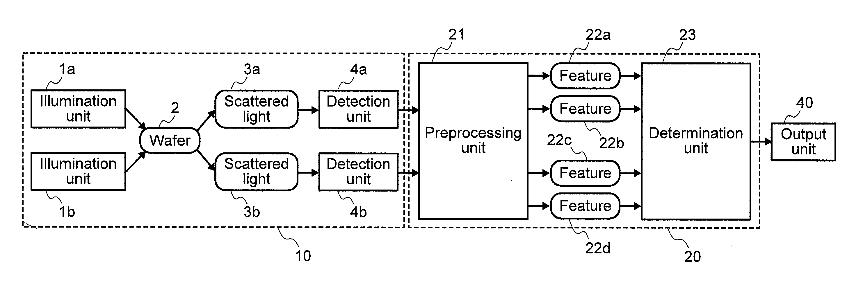
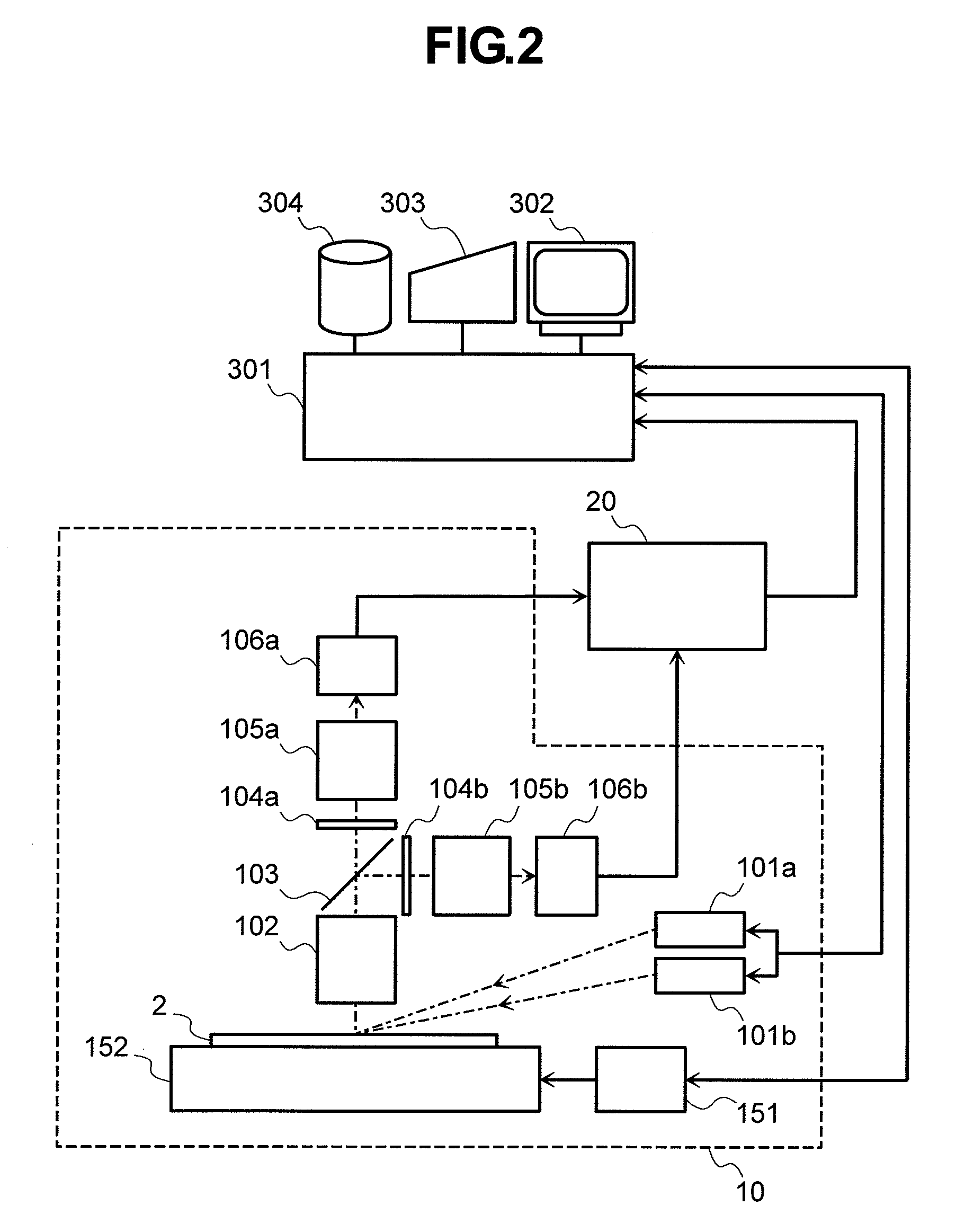
[0037]Embodiments of the present invention will be described using FIG. 1 to FIG. 20. Below, explanations will be given taking as an example defect inspection on a semiconductor wafer.

[0038]FIG. 1 shows a configuration of the present invention. An optical unit 10 is constructed with a plurality of illumination units 1a, 1b and a plurality of detection units 4a, 4b. The illumination units 1a, 1b irradiate mutually different illumination light to an inspection subject substrate 2. Illumination light coming from the respective illumination units 1a, 1b generate scattered light 3a, 3b, which are detected by the respective detection units 4a, 4b as scattered light intensity signals. The detected scattered light intensity signals are inputted into a processing unit 20. The processing unit 20 is made up of a preprocessing unit 21 and a determination unit 23. The plurality of scattered light intensity signals detected by the optical unit 10 are inputted into the preprocessing unit 21. The p...


PUM

PropertyMeasurementUnit
sizeaaaaaaaaaa
sizeaaaaaaaaaa
sizeaaaaaaaaaa

Abstract

In an inspection subject substrate, there is a problem that a defect signal is overlooked due to scattered light from a pattern and sensitivity decreases in an irregular circuit pattern part. The inventors propose a defect inspection method, characterized by comprising: an illumination step of guiding light emitted from a light source to a predetermined area on an inspection subject substrate under a plurality of predetermined optical conditions; a detection step of obtaining an electric signal by guiding scattered light components propagating in a predetermined range of azimuthal angle and in a predetermined range of elevation angle to a detector for each of a plurality of scattered light distributions occurred correspondingly to the plurality of optical conditions in the predetermined area; and a defect determination step of determining a defect based on the plurality of electric signals obtained in the detection step.

Description

[0001]The present application claims priority from Japanese application serial no. JP 2007-115005, filed on Apr. 25, 2007, the content of which is hereby incorporated by reference into this application.BACKGROUND OF THE INVENTION[0002]1. Field of the Invention[0003]The present invention relates to a defect inspection system that in a manufacture process for manufacturing an object by forming a pattern on a substrate, such as a semiconductor manufacture process, a liquid crystal display device manufacture process, and a printed circuit board manufacture process, inspects an occurrence status of a defect, such as a foreign substance, in manufacture steps of detecting a defect occurred, such as a foreign substance, analyzing it, and taking action, and a method therefor.[0004]2. Description of the Related Art[0005]In the conventional semiconductor manufacture process, if a foreign substance exists on a semiconductor substrate (an inspection subject substrate to be examined) it will beco...

Claims


Application Information

Patent Timeline
Patent Type & Authority Applications(United States)
IPC IPC(8): G01N21/88
CPCG01N21/9501G01N21/95607G01N21/95623G01N2021/8896
Inventor URANO, YUTASAKAI, KAORUMAEDA, SHUNJI
Owner HITACHI HIGH-TECH CORP
Why Eureka
Try Eureka