Process for fabricating a structure for epitaxy without an exclusion zone

a technology of exclusion zone and structure, applied in the field of semiconductor materials, can solve the problems of mechanical weakening of seed layer, insufficient bonding force obtained on the periphery of assembly, and preventing good contact between support substrates, so as to reduce the roughness of potentially work-hardened zones

Inactive Publication Date: 2008-12-11
S O I TEC SILICON ON INSULATOR THECHNOLOGIES
View PDF10 Cites 37 Cited by
  • Summary
  • Abstract
  • Description
  • Claims
  • Application Information

AI Technical Summary

Benefits of technology

The patent describes how a method was developed for making highly precise layers of semiconductor materials. This involves shaping the surface of the material with very high precision through both sides, smoothing it to remove any uneven surfaces or potential damage from previous processing steps, and then removing some of the outer edge of the material to achieve a smooth transition between different parts of the device. These techniques result in better quality semiconductor materials that are more suitable for use in electronic devices like computers and phones.

Problems solved by technology

The technical problem addressed in this patent is how to produce high quality semiconductor materials through the use of composite structures made up of different layers grown via epitaxis. These composites can include materials of groups III/V, VI, VII, VIII, and IV, among others. However, current methods often result in incomplete transfer of all parts of the original donor substrate's crystal structure onto the recipient substrate due to issues like edge rounding and poor surface contact, leading to wasted material and increased costs associated with reusing the donor substrate. Additionally, some applications require large amounts of expensive starting materials to achieve the desired size of the final product. There is also difficulty in achieving optimal adhesion between the various layers without causing damage to the substrates.

Method used


Image

  • Process for fabricating a structure for epitaxy without an exclusion zone
  • Process for fabricating a structure for epitaxy without an exclusion zone
  • Process for fabricating a structure for epitaxy without an exclusion zone

Examples


Embodiment Construction

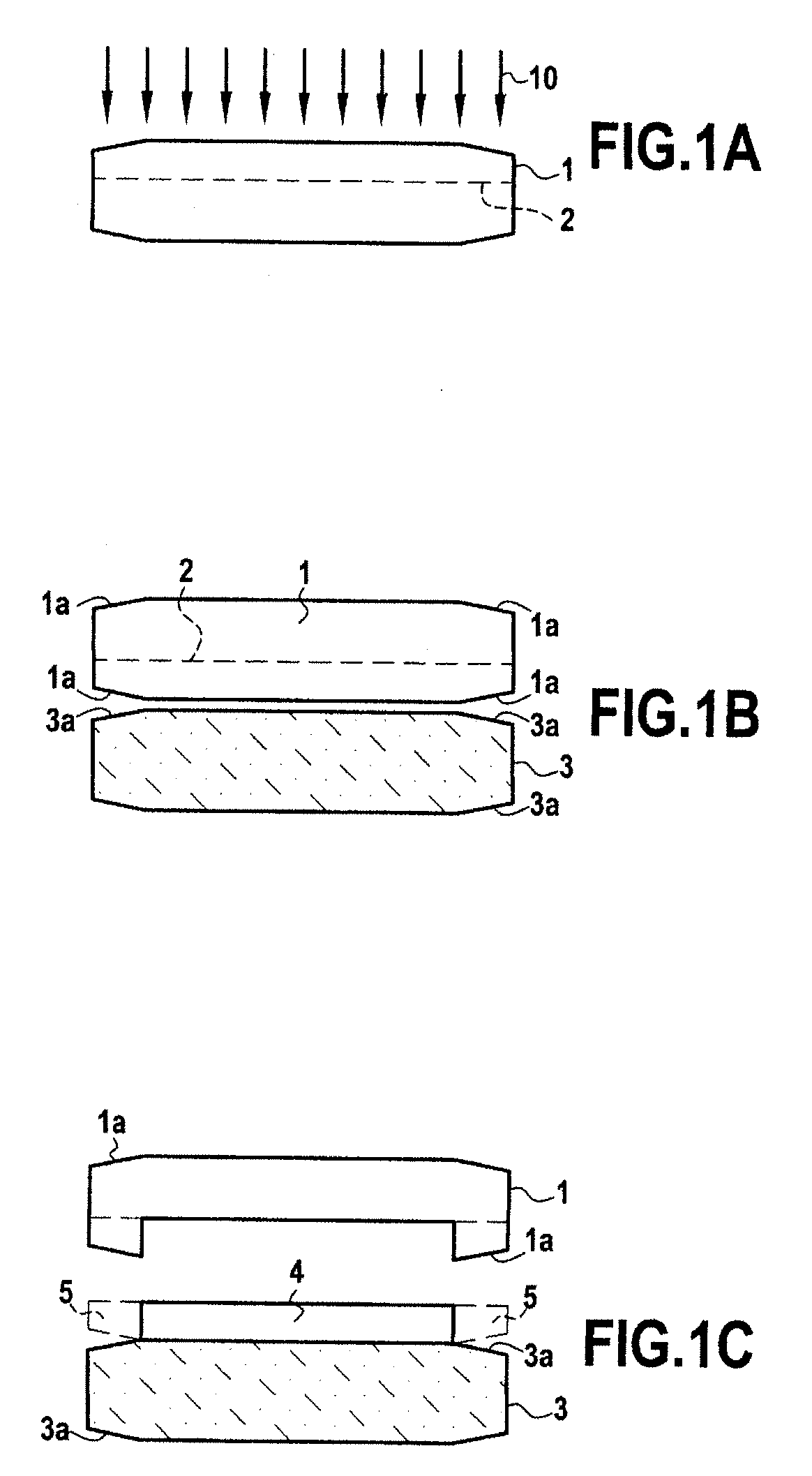
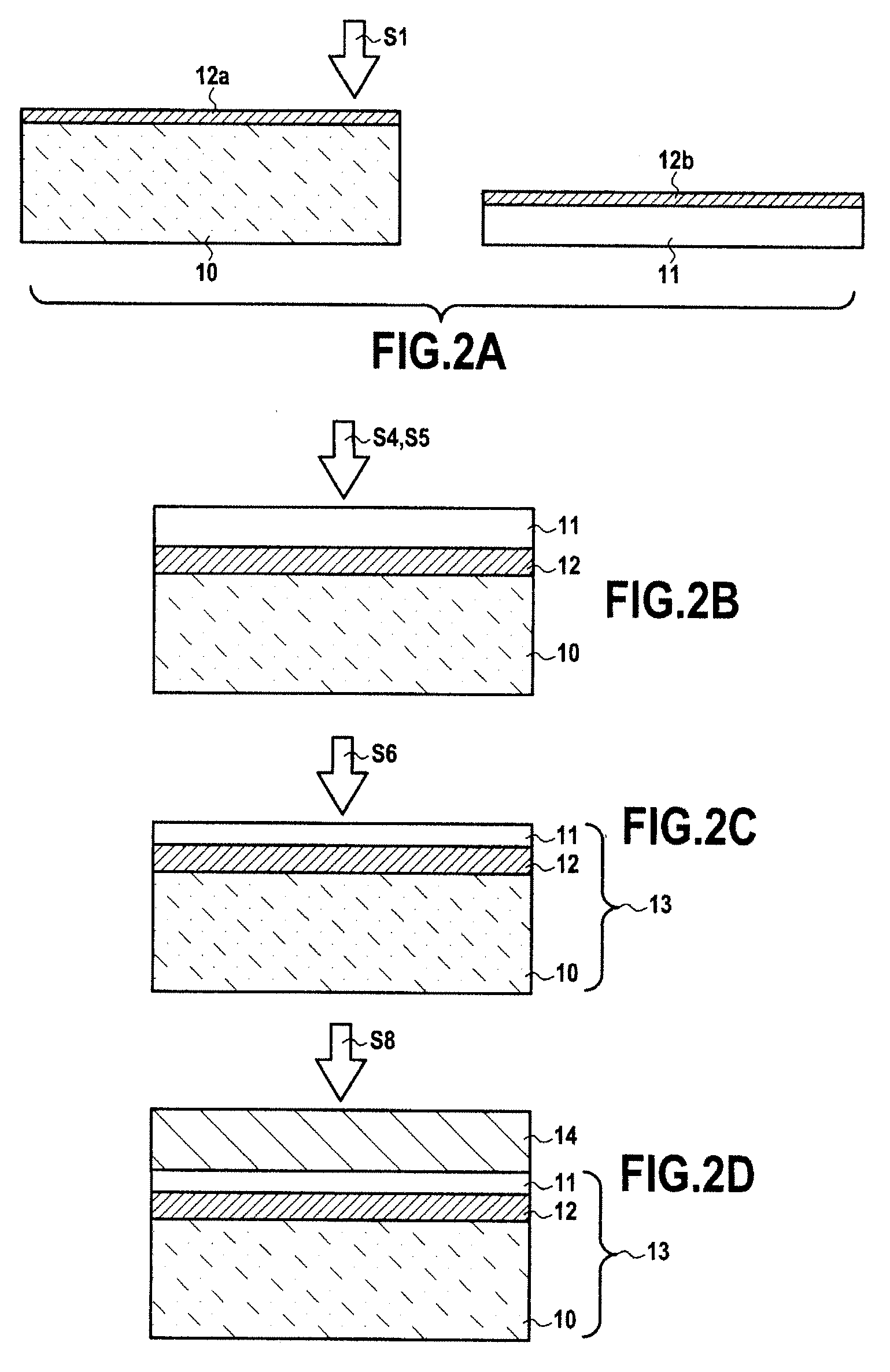
[0038]The present invention applies in general to the production of layers of semiconductor materials, in particular III / V, III / N and IV materials, by epitaxy in the form of wafers, these layers having, directly after their formation by epitaxy, a specified wafer diameter. For this purpose, the present invention proposes a process for producing a composite structure for epitaxy starting from wafers having a chamfer or “edge rounding” zone, which process nevertheless makes it possible to produce epitaxially grown layers of semiconductor material without loss of diameter compared to the initial diameter of the wafer used to form the crystalline growth seed layer. As described below, the composite structure for epitaxy according to the invention comprises at least a support substrate and a crystalline growth seed layer of semiconductor material.

[0039]The material of the support substrate may be chosen so as to have a thermal expansion coefficient (TEC) close to that of the semiconducto...


PUM

PropertyMeasurementUnit
Thicknessaaaaaaaaaa
Thicknessaaaaaaaaaa
Diameteraaaaaaaaaa

Abstract

A process for fabricating a composite structure for epitaxy, including at least one crystalline growth seed layer of semiconductor material on a support substrate, with the support substrate and the crystalline growth seed layer each having, on the periphery of their bonding face, a chamfer or an edge rounding zone. The process includes at least one step of wafer bonding the crystalline growth seed layer directly onto the support substrate and at least one step of thinning the crystalline growth seed layer. After thinning, the crystalline growth seed layer has a diameter identical to its initial diameter.

Description


Claims


Application Information

Patent Timeline
Owner S O I TEC SILICON ON INSULATOR THECHNOLOGIES
Why Eureka
Try Eureka