Plasma processing apparatus

a processing apparatus and plasma technology, applied in the direction of coatings, chemical vapor deposition coatings, electric discharge tubes, etc., can solve the problems of non-linear characteristics, design rule constraints on features, and the conventional oxide film etching method is, therefore, not good enough to satisfy the demands of the market, so as to suppress the unevenness of the electric field and achieve the effect of uniform plasma density, uniform plasma density, and uniform plasma density

Inactive Publication Date: 2008-12-18
TOKYO ELECTRON LTD
View PDF27 Cites 21 Cited by
  • Summary
  • Abstract
  • Description
  • Claims
  • Application Information

AI Technical Summary

Benefits of technology

[0021]In the plasma processing apparatus of the present invention, high frequency electric power is applied to the first electrode. There is provided a harmonic absorbing member for absorbing a harmonic of the high frequency electric power source so as to come into contact with a peripheral portion or circumference of a face of the first electrode, which is opposite to the second electrode. The harmonic absorbing member absorbs a harmonic reflected from plasma before the h

Problems solved by technology

There are also design rule constraints on features like the contact hole.
The conventional oxide film etching method is, therefore, beginning to be not good enough to satisfy the demands of the market.
Further, such a higher density of the plasma by the higher frequency remarkably causes non-linear characteristics of the plasma, so that a harmonic may be easily interposed on the reflected wave form the plasma.
If the electric field is made uneven in such a manner, the density of plasma will be also made uneven, with the result that the etching rate of etching will be uneven.
The above-mentioned problems in generating a high-density plasma, however, have not been recognized clearly, and thus a proposal for preventing the above-mentioned uneven electric field has not sufficiently been pr

Method used


Image

  • Plasma processing apparatus
  • Plasma processing apparatus
  • Plasma processing apparatus

Examples


first embodiment

[0045]FIG. 1 is a sectional view schematically showing the plasma etching apparatus according to the present invention.

[0046]A plasma processing apparatus 1 is constituted as a capacitive coupling type parallel plate etching apparatus having two electrode plates being opposed to each other (arranged in parallel and facing each other) one of which is connected to a plasma generating electric power source.

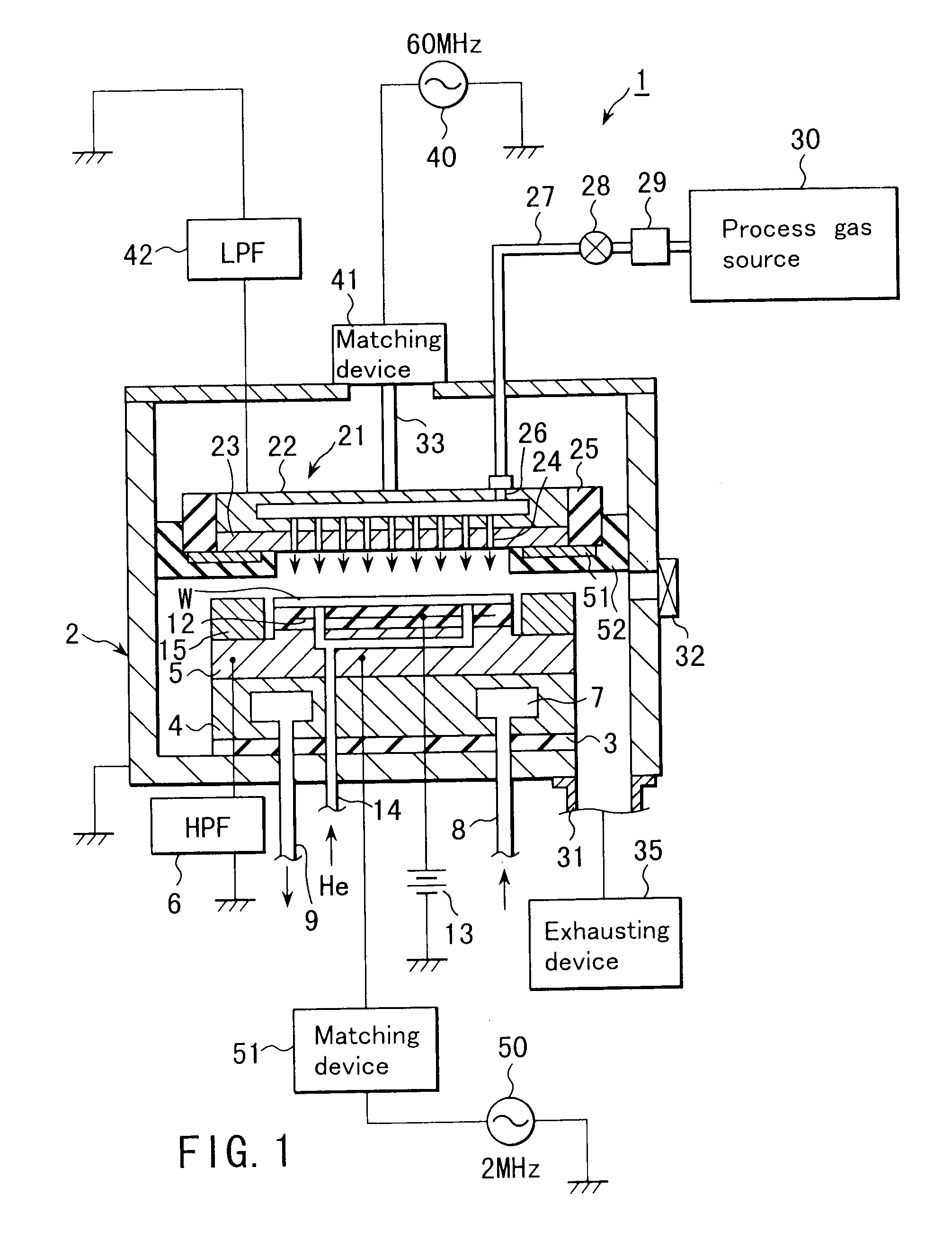
[0047]The plasma processing apparatus 1 has a chamber 2 formed of aluminum in a cylinder shape the surface of which is processed (subjected to an anodic oxidation process) to form alumite. The chamber 2 is grounded.

[0048]The chamber 2 is provided on the bottom face with an insulator 3, such as a ceramic, upon which a suscepter supporting body 4 formed in a substantially columnar shape is placed, for mounting an object to be processed, such as a semiconductor wafer (hereinafter referred to as “wafer”) W. There is further provided on the suscepter supporting body 4 a suscepter 5 consti...

second embodiment

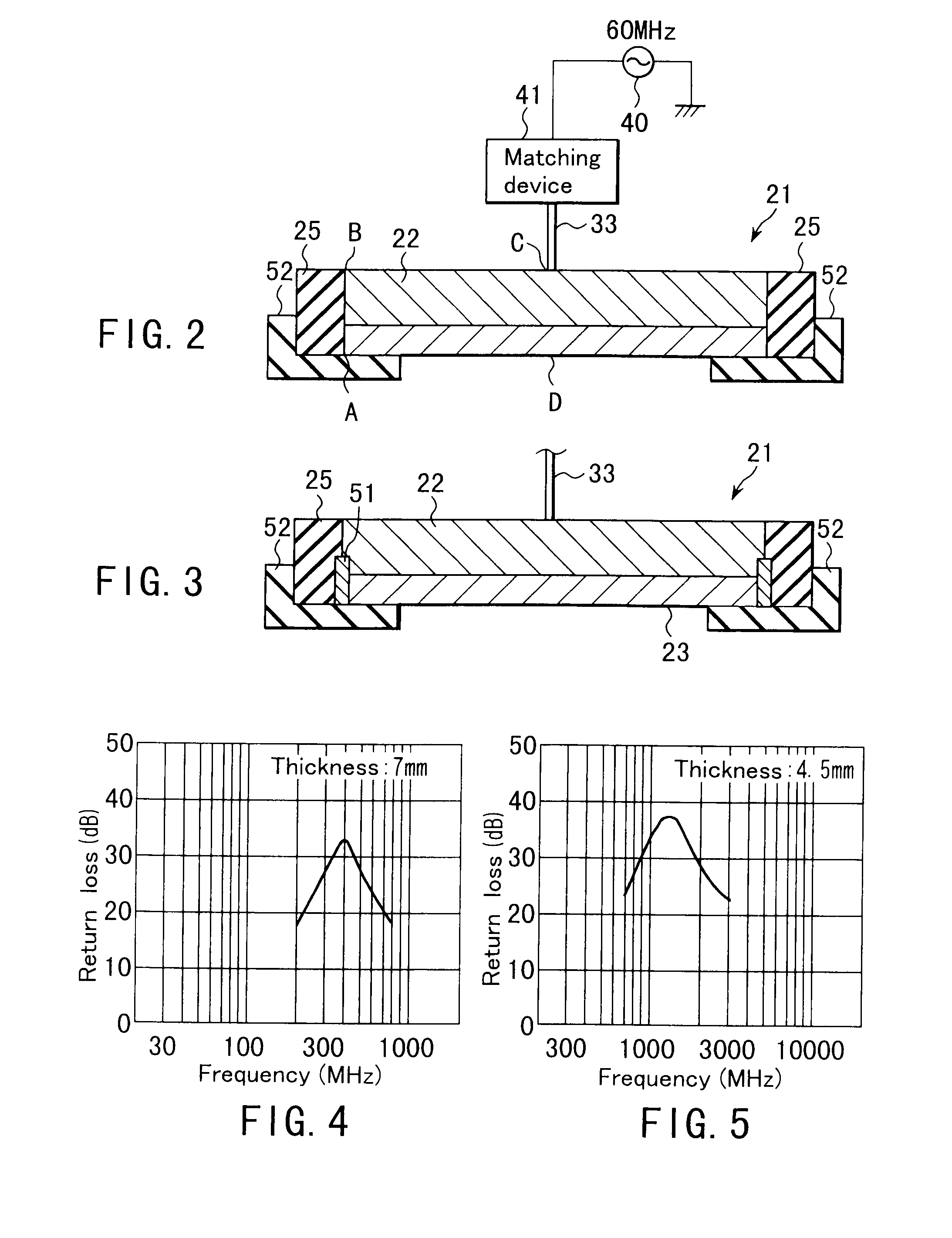
[0124]The above-mentioned first to sixth examples of the upper electrodes in the second embodiment is effective particularly in the case where the frequency of the electric power applied to the electrode is 27 MHz or more, and the density of plasma is as high as 1×10¹¹ / cm3 or higher.

[0125]Next, the etching apparatus according to the second embodiment will be described about the example in which an oxide film formed on the wafer W is etched.

[0126]As in the first embodiment, the wafer W is transferred into the chamber 2 to be electrostatically attached to an electrostatic chuck 11. After the pressure of the chamber 2 is reduced to a predetermined level, the process gas is introduced into the chamber 2 to be blown to the wafer W under a predetermined pressure.

[0127]Subsequently, a high frequency electric power having frequency of 60 MHz is applied to the upper electrode 21 from the high frequency electric power source 40. By applying such a high frequency electric power, a high frequen...

fourth embodiment

[0147]the present invention will be described below.

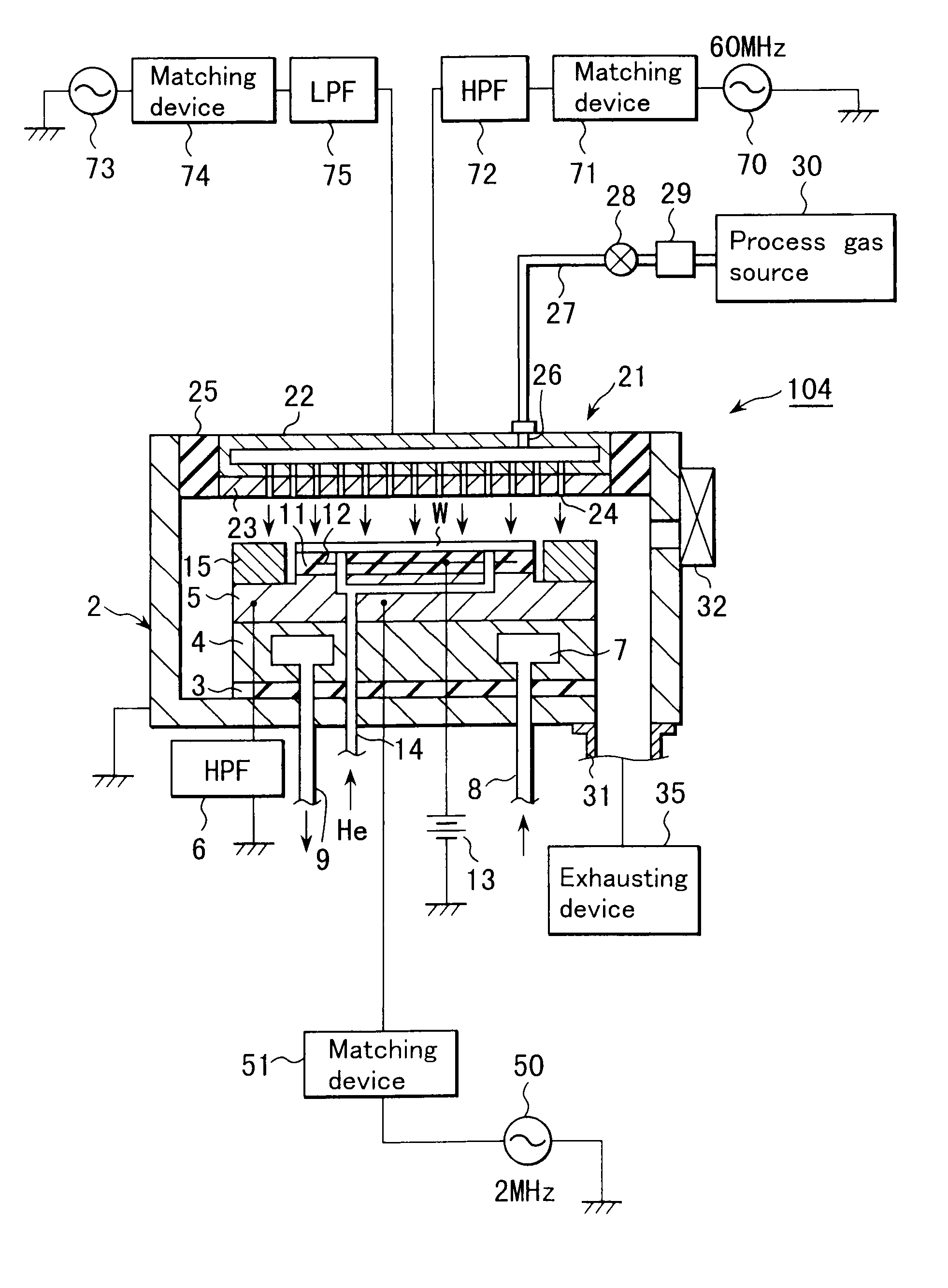
[0148]FIG. 18 shows an example of a constitution of a plasma processing apparatus according to the fourth embodiment of the present invention, used as a capacity coupling parallel plate etching apparatus. The same constituent elements as those of the second embodiment shown in FIG. 16 are denoted by the same symbols and the description thereof is omitted.

[0149]In the etching apparatus 104, the upper electrode 21 is connected to two high frequency electric power sources. One is the first high frequency electric power source 70 for generating plasma connected to the upper electrode 21 via a high pass filter (HPF) 72 and a matching device 71. The other is the second high frequency electric power source 73 connected to the upper electrode 21 via a low pass filter (LPF) 75 and a matching device 74.

[0150]The first high frequency electric power source 70 has a high frequency of 27 MHz or higher. By applying electric power having such a hi...


PUM

PropertyMeasurementUnit
Frequencyaaaaaaaaaa
Thicknessaaaaaaaaaa
Densityaaaaaaaaaa

Abstract

In the plasma processing apparatus of the present invention, a first electrode for connecting a high frequency electric power source in a chamber is arranged to be opposed to a second electrode. A substrate (W) to be processed is placed between the electrodes. There is provided a harmonic absorbing member for being able to absorb harmonics of the high frequency electric power source so as to come in contact with a peripheral portion or circumference of a face of the first electrode 21, which is opposite the second electrode. The harmonic absorbing member absorbs the reflected harmonic before the harmonic returns to the high frequency electric power source. By absorbing the harmonic in this manner, the standing wave due to the harmonic will be effectively prevented from being generated, and the density of plasma is made even.

Description

CROSS-REFERENCE TO RELATED APPLICATIONS[0001]This application is a divisional of and claims the benefit of U.S. application Ser. No. 09 / 959,745, filed Nov. 5, 2001, which is a National Stage application of PCT / JP00 / 02770, filed Apr. 27, 2000, and claims priority to Japanese Patent Application Nos. 11-125637, filed May 6, 1999; 11-126878, filed May 7, 1999; 11-129696, filed May 11, 1999 and 11-141209, filed May 21, 1999. The entire content of each of these applications is incorporated herein by reference to the extent that such incorporation does not create an issue of new matter.TECHNICAL FIELD[0002]The present invention relates to a plasma processing apparatus for performing etching and film forming on a substrate such as a semiconductor substrate by plasma processing.BACKGROUND ART[0003]In a process for manufacturing semiconductor devices, various plasma processing such as etching, film forming by sputtering or CVD film forming (Chemical Vapor Depositing) have been frequently empl...

Claims


Application Information

Patent Timeline
IPC IPC(8): C23C16/00H01J37/32
CPCH01J37/32082H01J37/321H01J37/32165H01J37/3255H01J2237/3323H01L21/3065
Inventor KOSHIISHI, AKIRAHIROSE, KEIZO
Owner TOKYO ELECTRON LTD
Why Eureka
Try Eureka