
Method for eliminating duo loading effect using a via plug

a technology of duo loading and via plug, which is applied in the direction of semiconductor devices, semiconductor/solid-state device details, electrical equipment, etc., can solve the problems of dual damascene etching, high cost of ic fabrication facilities, and high cost of devices. , to achieve the effect of reducing the duo loading effect, and reducing the pattern diversity of integrated circuits

Active Publication Date: 2008-12-18
SEMICON MFG INT (SHANGHAI) CORP
View PDF5 Cites 8 Cited by
  • Summary
  • Abstract
  • Description
  • Claims
  • Application Information

AI Technical Summary

Benefits of technology

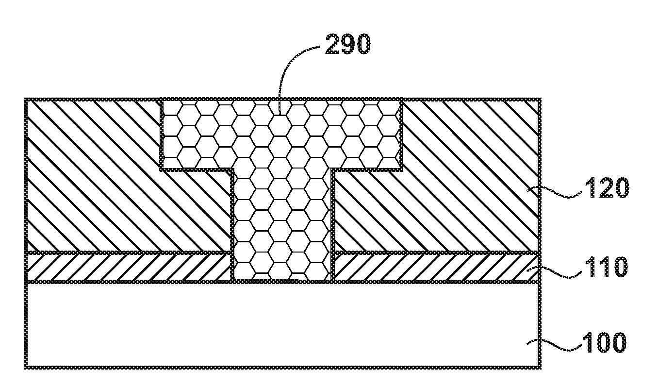
[0017]It is to be appreciated that uniformity of depth on a semiconductor according to the present invention reduces the DUO loading effect. Among other things, the present invention reduces the DUO loading effect by reducing pattern diversity in integrated circuits. It is also to be appreciated that the present invention has a wide range of application. For example, the present invention allows better uniformity and consistency in semiconductor fabrication.

Problems solved by technology

An IC fabrication facility can cost hundreds of millions, or even billions, of dollars.
Making devices smaller is very challenging, as each process used in IC fabrication has a limit.
Among various types of etching processes, dual damascene etching has been one of the most difficult.
Due to the complexity associated with dual damascene, the standard for both etching and striping processes are often strict.
Often, the margin for error is typically very small.
One of the challenge associated with using the DUO material is to reduce or eliminate loading effect caused by pattern diversity.
Unfortunately, conventional techniques are often inadequate for many manufacturing needs of semiconductors.
For example, DUO material used in conventional techniques often cause too much loading effect.

Method used


Image

  • Method for eliminating duo loading effect using a via plug
  • Method for eliminating duo loading effect using a via plug
  • Method for eliminating duo loading effect using a via plug

Examples


Embodiment Construction

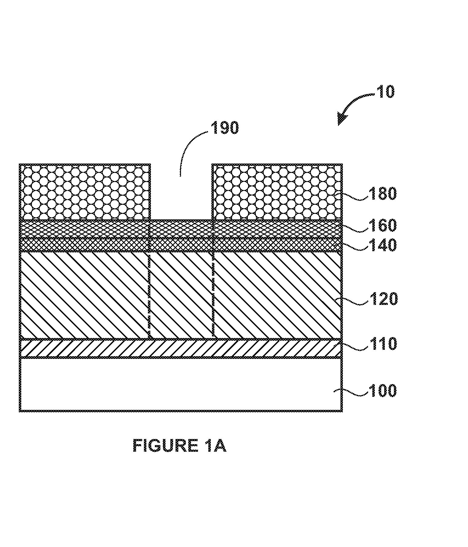
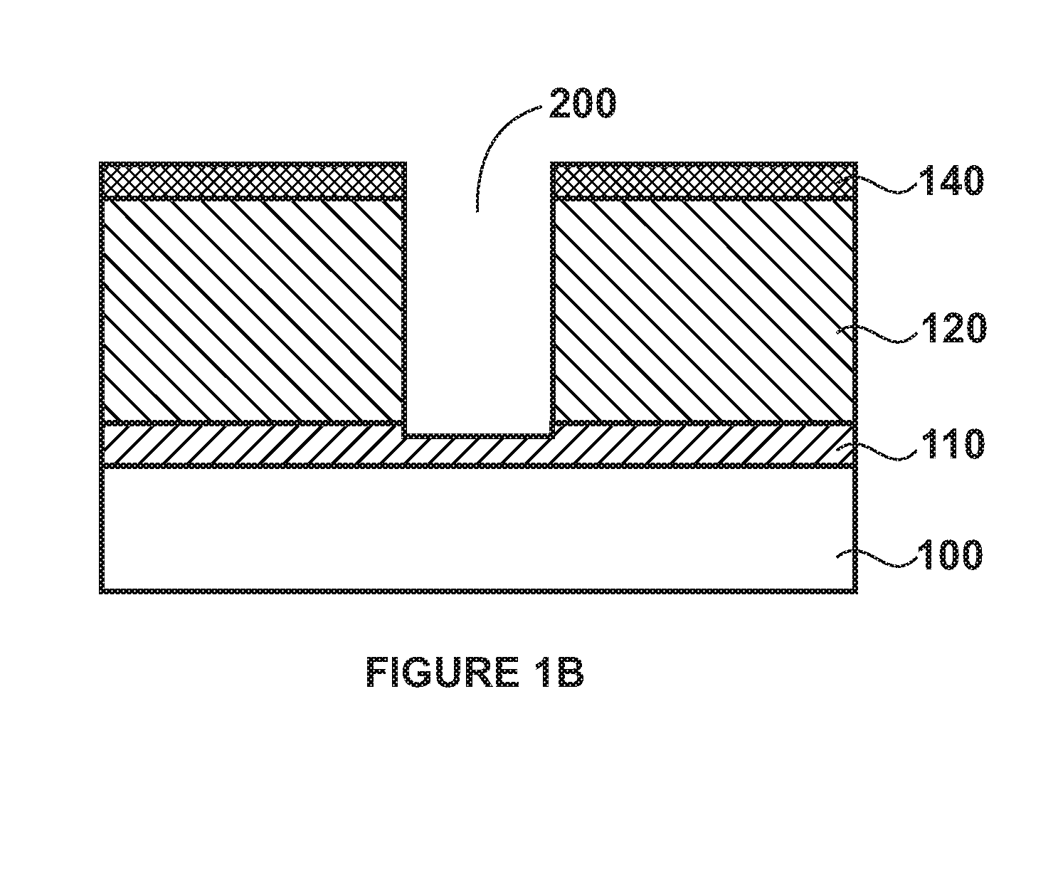
[0022]The present invention is directed to integrated circuits and their processing for the manufacture of semiconductor devices. More particularly, the invention provides a method and device for the etching process for the manufacture of integrated circuits. Merely by way of example, the invention has been applied to dual-damascene formation. But it would be recognized that the invention has a much broader range of applicability.

[0023]In the past, conventional techniques have been using deep ultraviolet light absorbing oxide (DUO) materials to fill via during the manufacturing process. For example, the DUO material is used in this application as a sacrifice layer. One of the challenge associated with using the DUO material is to reduce or eliminate loading effect caused by pattern diversity. Unfortunately, conventional techniques are often inadequate for many manufacturing needs of semiconductors. For example, DUO material used in conventional techniques often cause too much loadin...


PUM


Abstract

Method for eliminating loading effect using a via plug. According to an embodiment, the present invention provides a method of processing an integrated circuit wherein a loading effect is reduced. The method includes a step for providing a substrate, which is characterized by a first thickness. The method also includes a stop for forming an inter metal dielectric layer overlaying the substrate. The inter metal dielectric layer is characterized by a second thickness. The method additionally includes a step for forming a first photoresist layer overlaying the inter metal dielectric layer. The first photoresist layer is associated with a first pattern. Additionally, the method includes a step for forming a first opening positioned at least partially inside the inter metal dielectric layer. The first via opening is characterized by a first depth. The method additionally includes a step for removing the first photoresist layer. The method further includes a step for forming a via plug.

Description

CROSS-REFERENCES TO RELATED APPLICATIONS[0001]This application claims priority to Chinese Patent No. 200710042145.8, filed Jun. 18, 2007 (SMIC Docket No. 1-05-196), commonly assigned and hereby incorporated by reference for all purposes.BACKGROUND OF THE INVENTION[0002]The present invention is directed to integrated circuits and their processing for the manufacture of semiconductor devices. More particularly, the invention provides a method and device for the etching process for the manufacture of integrated circuits. Merely by way of example, the invention has been applied to dual-damascene formation and reduces loading effects that are typically associated with pattern diversity. But it would be recognized that the invention has a much broader range of applicability.[0003]Integrated circuits or “ICs” have evolved from a handful of interconnected devices fabricated on a single chip of silicon to millions of devices. Current ICs provide performance and complexity far beyond what was...

Claims


Application Information

Patent Timeline
Patent Type & Authority Applications(United States)
IPC IPC(8): H01L23/48H01L21/44
CPCH01L21/76808
Inventor XIANGHUI, WUMA, CHING-TIENSHEN, MAN HUASHAN, CHI YU
Owner SEMICON MFG INT (SHANGHAI) CORP
Learn More