

High accuracy current mode duty cycle and phase placement sampling circuit
- Summary
- Abstract
- Description
- Claims
- Application Information
AI Technical Summary
Problems solved by technology
Method used
Image

Examples
Embodiment Construction
[0020]A duty cycle and phase placement sampling circuit 401 according to one embodiment of the invention is shown in FIG. 4. The circuit comprises a precharge retiming circuit 402 and a differential input sampler 403 with replicated differential pair stages 404 and 405 to accommodate two sets of differential inputs.
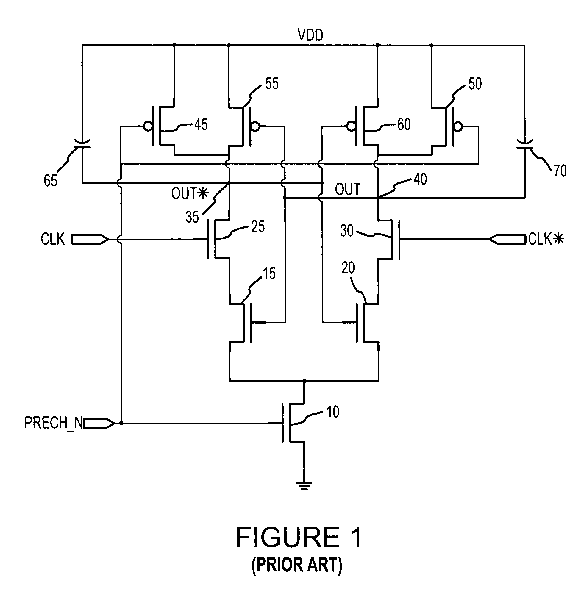
[0021]With reference to FIG. 4, primary input stage 404 consists of six NMOS transistors. NMOS transistor 413 is a bias transistor which limits the current through the primary input stage 404. This transistor may be biased by a bias signal applied to the BIAS input 430. Such a signal may be provided by, for example, an external current mirror as is understood by those of ordinary skill in the art. Immediately above the bias NMOS 413 is an enable transistor 414 which is controlled by the active-low precharge signal PreChargeA 431. When the PreChargeA signal is asserted, the enable transistor 414 is turned off and prevents current flow through the NMOS 413 down to ground. I...
PUM
 Abstract
Description
Claims
Application Information