
Reflection-Repressed Wire-Grid Polarizer

a polarizer and reflection-repression technology, applied in the field of inorganic wiregrid polarizers, can solve the problems of significant cost and weight, polarizers that have not been successfully extended, and poor service of visible spectrum by this technology

Inactive Publication Date: 2008-12-25
MOXTEK INC
View PDF99 Cites 85 Cited by
  • Summary
  • Abstract
  • Description
  • Claims
  • Application Information

AI Technical Summary

Benefits of technology

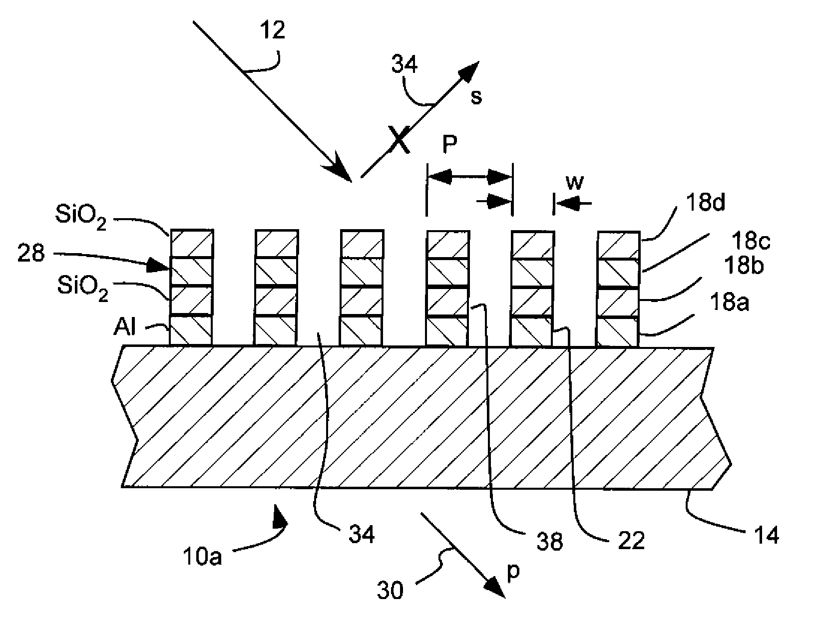
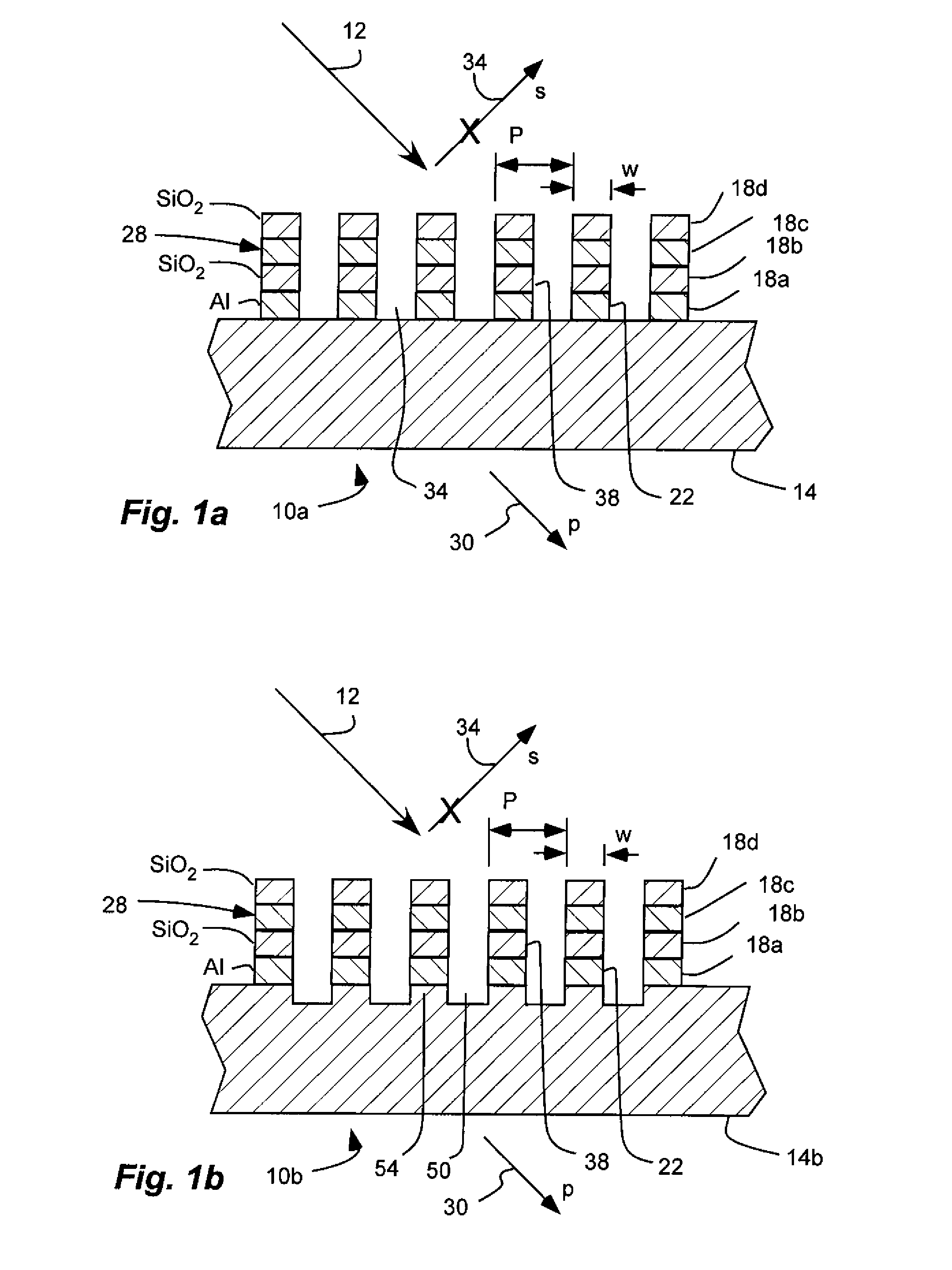
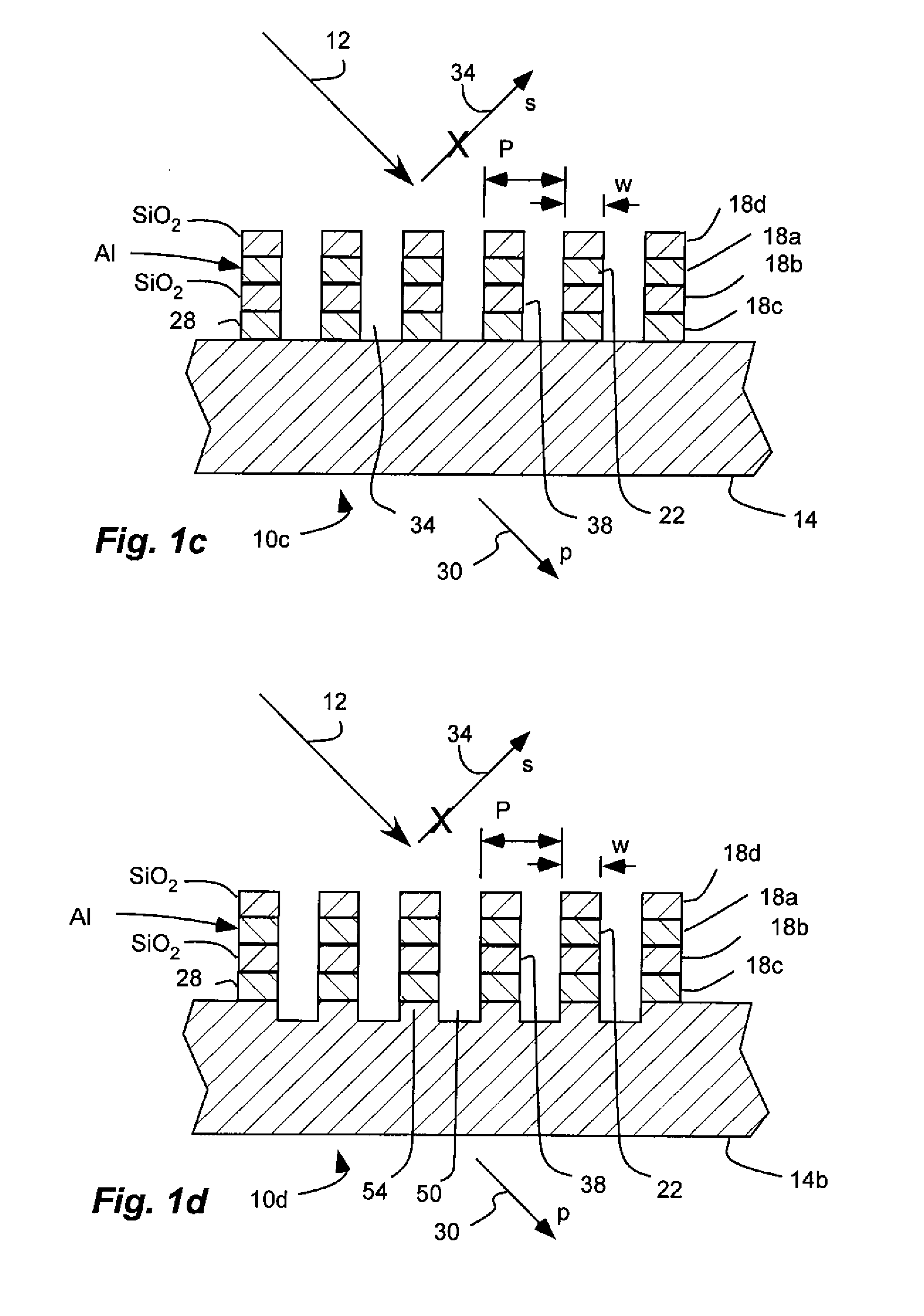
The present invention provides an inorganic polarizer that has high transmission of orthogonally polarized light, with a contrast greater than 500:1 in each of the three primary colors of blue, green, and red. The polarizer has a reasonable acceptance angle and can be made in a plate format. It can be manufactured at a reasonable cost for use in the competitive display market. The polarizer has a reflection-repressing layer that includes an inorganic and non-dielectric material that absorbs visible or infrared light. A dielectric layer is used to separate the polarizing wire-grid layer from the absorptive layer, and includes an inorganic and dielectric material. The polarizer has a high degree of reflection repression, meaning it minimizes the reflection of light.

Problems solved by technology

Such MacNeille PBSs generate no astigmatism, but have a narrow acceptance angle, and have significant cost and weight.
However, this type of polarizer has not successfully been extended into the green and blue portions of the visible spectrum, leaving the visible spectrum poorly served by this technology.
Because of the optical design of such systems, it is difficult for them to use reflective polarizers in the image-bearing part of the optical path.
The first is that light reflected back into the display panels is known to cause the transistors in the drive circuitry on the panel to be inoperable due to the photoelectric effect disturbing the transistors operation.
The second problem is that the reflected light can cause ghost images and cause a loss of contrast in the image on the screen.
Over time, as these displays have become brighter, such polarizers have become a weak point in the system, leading to concerns about early failure of the polarizers.
Continued progress in the display market towards brighter and less-expensive displays means that the time will soon come that such solutions will no longer be practical.

Method used


Image

  • Reflection-Repressed Wire-Grid Polarizer
  • Reflection-Repressed Wire-Grid Polarizer
  • Reflection-Repressed Wire-Grid Polarizer

Examples


example 1

[0053]Referring to FIG. 2a, a first non-limiting example of a reflection repressed, wire-grid polarizer 10f is shown configured for use in the infrared spectrum.

[0054]The polarizer 10f has four layers disposed over a substrate 14 including a polarizing layer 18a, a reflection-repressing layer 18c, a dielectric layer 18b separating the polarizing and reflection-repressing layers, and a second dielectric layer 18d separated from the first dielectric layer 18b by the reflection-repressing layer. The substrate is glass, such as BK7 glass. The first layer or polarizing layer 18a is disposed on the substrate. The polarizing layer 18a is an array of parallel metal wires 22 formed of aluminum (AL) with a period P of 144 nm. The polarizing layer 18a has a thickness of 77 nm. The reflection-repressing layer 18c is formed of niobium siliside (NbSi; n≈3.8, k≈2.90 at 1550 nm) and has a thickness of 50 nm. The first and second dielectric layers 18b and 18d are formed of silicon dioxide (SiO2) and...

example 2

[0056]Referring to FIG. 3a, a second non-limiting example of a reflection repressed, wire-grid polarizer 10g is shown configured for use in the visible spectrum.

[0057]The polarizer 10g has four layers disposed over a substrate 14 including a polarizing layer 18a, a reflection-repressing layer 18c, a dielectric layer 18b separating the polarizing and reflection-repressing layers, and a second dielectric layer 18d separated from the first dielectric layer 18b by the reflection-repressing layer. The substrate is glass, such as BK7 glass. The first layer or polarizing layer 18a is disposed on the substrate. The polarizing layer 18a is an array of parallel metal wires 22 formed of aluminum (AL) with a period P of 144 nm. The polarizing layer 18a has a thickness of 170 nm. The reflection-repressing layer 18c is formed of silicon (Si; n≈4.85, k≈0.8632 at 550 nm) and has a thickness of 12 nm. The first and second dielectric layers 18b and 18d are formed of silicon dioxide (SiO2) and have a ...

example 3

[0059]Referring to FIG. 4a, a third non-limiting example of a reflection repressed, wire-grid polarizer 10h is shown configured for use in the visible spectrum.

[0060]The polarizer 10b has four layers disposed over a substrate 14 including a polarizing layer 18a, a reflection-repressing layer 18c, a dielectric layer 18b separating the polarizing and reflection-repressing layers, and a second dielectric layer 18d separated from the first dielectric layer 18b by the reflection-repressing layer. The substrate is glass, such as BK7 glass. The first layer or polarizing layer 18a is disposed on the substrate. The polarizing layer 18a is an array of parallel metal wires 22 formed of aluminum (AL) with a period P of 144 nm. The polarizing layer 18a has a thickness of 170 nm. The reflection-repressing layer 18c is formed of tantalum (Ta; n≈2.95, k≈3.52 at 550 nm) and has a thickness of 13 nm. The first and second dielectric layers 18b and 18d are formed of silicon dioxide (SiO2) and have a th...


PUM


Abstract

A reflection repressed wire-grid polarizer device for polarizing incident visible or infrared light and selectively repressing a reflected polarization includes at least three layers disposed on a substrate. A polarizing wire-grid layer has an array of parallel metal wires with a period less than half the wavelength of the incident light. A reflection-repressing layer or grid includes an inorganic and non-dielectric material which is optically absorptive of visible or infrared light. A dielectric layer or grid includes an inorganic and dielectric material.

Description

RELATED APPLICATIONS[0001]This is related to U.S. patent application Ser. No. ______, filed Jun. 22, 2007, as TNW Docket No. 00546-23945.CIP entitled “Selectively Absorptive Multilayer Wire-Grid Polarizer”; and U.S. patent application Ser. No. 11,005,927, filed Dec. 6, 2004; which are herein incorporated by reference.BACKGROUND[0002]1. Field of the Invention[0003]The present invention relates generally to an inorganic wire-grid polarizer which has been configured to substantially repress the reflected polarization while substantially transmitting the orthogonal polarization with particular focus on the use of such a polarizer for use in the visible and infra-red portion of the electromagnetic spectrum.[0004]2. Related Art[0005]Various types of polarizers or polarizing beam splitters (PBS) have been developed for polarizing light, or separating orthogonal polarization orientations of light. A MacNeille PBS is based upon achieving Brewster's angle behavior at the thin film interface a...

Claims


Application Information

Patent Timeline
Patent Type & Authority Applications(United States)
IPC IPC(8): G02B5/30
CPCG02B5/3058
Inventor WANG, BINGARDNER, ERICPERKINS, RAYMOND T.
Owner MOXTEK INC
Learn More