Semiconductor device and method of manufacturing the same

a semiconductor and semiconductor technology, applied in semiconductor lasers, solid-state devices, lasers, etc., can solve the problems of easy deterioration, cracking of deterioration of adhesion between light emitting elements and light detecting elements, so as to achieve efficient reflection of spontaneous emission light

Active Publication Date: 2009-01-01
SONY CORP
View PDF2 Cites 16 Cited by
  • Summary
  • Abstract
  • Description
  • Claims
  • Application Information

AI Technical Summary

Benefits of technology

[0009]To solve the disadvantage, there is a method of providing a control layer having a light transmission part in an area corresponding to a light emission area of a light emitting element between the light emitting element and a light detecting element and metal part having high reflectance around the light transmission part, and efficiently reflecting spontaneous emission light by the metal part having high reflectance.

Problems solved by technology

However, in the case of providing the control layer having such a metal part between the light emitting element and the light detecting element, the light emitting element and the light detecting element may not be formed in a lump by crystal growth on the same substrate.
However, when pressure is increased to improve adhesion between the light emitting element and the light detecting element, there is the possibility that a defect such as a crack occurs in the light emitting element and the light detecting element.
When the pressure is decreased to prevent occurrence of a defect such as a crack in the light emitting element and the light detecting element, there is the possibility that adhesion between the light emitting element and the light detecting element deteriorates.
As described above, the conventional method has a disadvantage such that the yield easily deteriorates in the process of adhering the light emitting element and the light detecting element.
Such a disadvantage always occurs at the time of adhering the elements to each other.

Method used


Image

  • Semiconductor device and method of manufacturing the same
  • Semiconductor device and method of manufacturing the same
  • Semiconductor device and method of manufacturing the same

Examples


first embodiment

Modification of First Embodiment

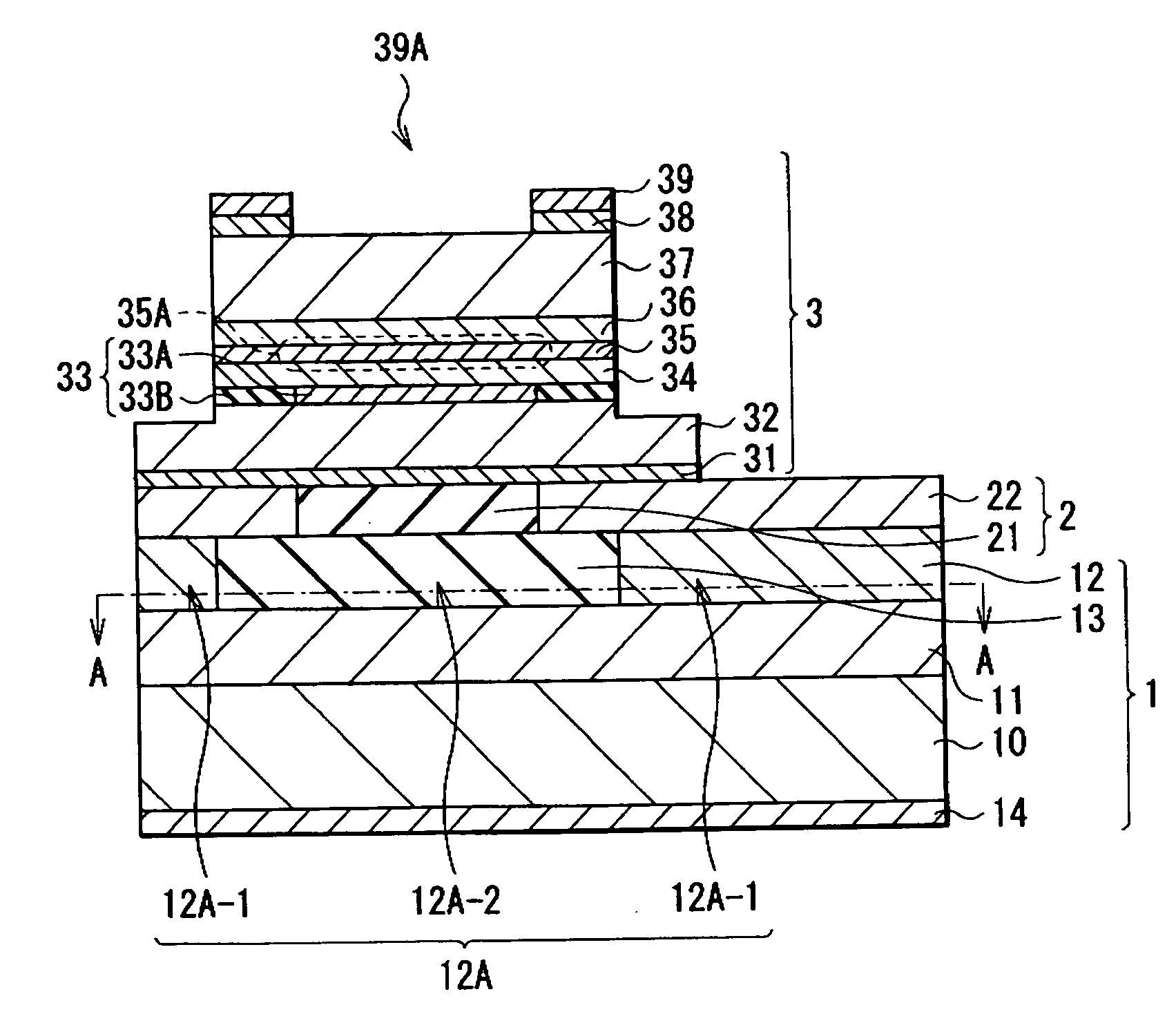
[0084]In the foregoing embodiment, the p-type semiconductor part 12 and the resin part 13 are provided on the light detecting element 1 side. Alternately, they may be provided on the VCSEL 3 side, as shown in FIG. 13. Also in the case of providing the resin part 13 on the VCSEL 3 side, effects similar to those of the foregoing embodiment are produced. In this case, it is preferable to provide the p-type contact layer 15 between the contact layer 2 and the light absorption layer 11.

Second Embodiment

[0085]FIG. 14 shows the structure of a semiconductor light emitting device as a second embodiment of the present invention. FIG. 14 is a schematic diagram and dimensions and shapes in FIG. 14 are different from actual ones. In the following description, when the same reference numeral as that in the foregoing embodiment is used, it means that the component has the configuration and function similar to those of the component having the same reference numeral....

second embodiment

Modification of Second Embodiment

[0092]Although the p-side semiconductor part 12 and the resin part 13 are provided on the light detecting element 5 side in the foregoing embodiment, as shown in FIG. 15, they may be provided on the VCSEL 4. As described above, also in the case of providing the resin part 13 on the VCSEL 4 side, effects similar to those of the embodiment are produced. In this case, it is preferable to provide a p-type contact layer 18 between the control layer 2 and the light absorption layer 11.

[0093]Although the present invention has been described by the embodiments, the invention is not limited to the embodiments but can be variously modified.

[0094]For example, the case of using a GaAs-based compound semiconductor as the semiconductor material has been described in the foregoing embodiments, other materials such as a GaInP-based (red-based) material, an AlGaAs-based (infra-red-based) material, a GaN-based (blue-green-based) material, or the like may be also used....


PUM


Abstract

The present invention provides a semiconductor device realizing reduced occurrence of a defect such as a crack at the time of adhering elements to each other. The semiconductor device includes a first element and a second element adhered to each other. At least one of the first and second elements has a pressure relaxation layer on the side facing the other of the first and second elements, and the pressure relaxation layer includes a semiconductor part having a projection/recess part including a projection projected toward the other element, and a resin part filled in a recess in the projection/recess part.

Description

CROSS REFERENCE TO RELATED APPLICATIONS[0001]The present invention contains subject matter related to Japanese Patent Application JP 2007-110512 filed in the Japanese Patent Office on Apr. 19, 2007, the entire contents of which being incorporated herein by reference.BACKGROUND OF THE INVENTION[0002]1. Field of the Invention[0003]The present invention relates to a semiconductor device having a plurality of elements stacked and a method of manufacturing the same.[0004]2. Description of the Related Art[0005]Hitherto, in a semiconductor device for a use of an optical fiber, an optical disk, and the like, as part of an object of making the light output level of a semiconductor light emitting element assembled in the device constant, emission light of the light emitting element is detected by a light detecting mechanism. The light detecting mechanism may be constructed by, for example, a reflector that branches part of emission light and a light detecting element that detects the branched...

Claims


Application Information

Patent Timeline
Patent Type & Authority Applications(United States)
IPC IPC(8): H01L33/00H01L21/00H01S5/026H01S5/183H01S5/187
CPCH01S5/0262H01S5/0264H01S5/18375H01S5/18311H01S5/0425H01S5/04252
Inventor KODA, RINTAROARAKIDA, TAKAHIROMASUI, YUJIOKI, TOMOYUKI
Owner SONY CORP
Why Eureka
Try Eureka