Wireless IC device

a technology of integrated circuits and wires, applied in the field of wireless integrated circuit devices, can solve the problems of reduced gain, ic chip is not driven, and the antenna formed on the chip is also very small, and achieves the effect of increasing the antenna gain

Active Publication Date: 2009-01-01
MURATA MFG CO LTD
View PDF12 Cites 171 Cited by
  • Summary
  • Abstract
  • Description
  • Claims
  • Application Information

AI Technical Summary

Benefits of technology

[0007]To overcome the problems described above, preferred embodiments of the present invention provide a wireless IC device that has an increased antenna gain, that operates at a sufficient distance from a reader-writer, and that can be used in frequency bands higher than UHF band.

Problems solved by technology

However, since the wireless IC chip itself is very small, the antenna formed on the chip is also very small and has a reduced gain.
Accordingly, there is a problem in that the IC chip is not driven unless the IC chip is in very close proximity to a reader-writer.
However, since the antenna of the substrate is a closed loop, it is difficult to achieve impedance matching between the antenna coil of the wireless IC chip and the antenna of the substrate in frequency bands greater than the Ultra High Frequency (UHF) band, although it is possible to achieve a sufficient gain in lower frequency bands, such as about 13.65 MHz.

Method used


Image

  • Wireless IC device
  • Wireless IC device
  • Wireless IC device

Examples


first preferred embodiment

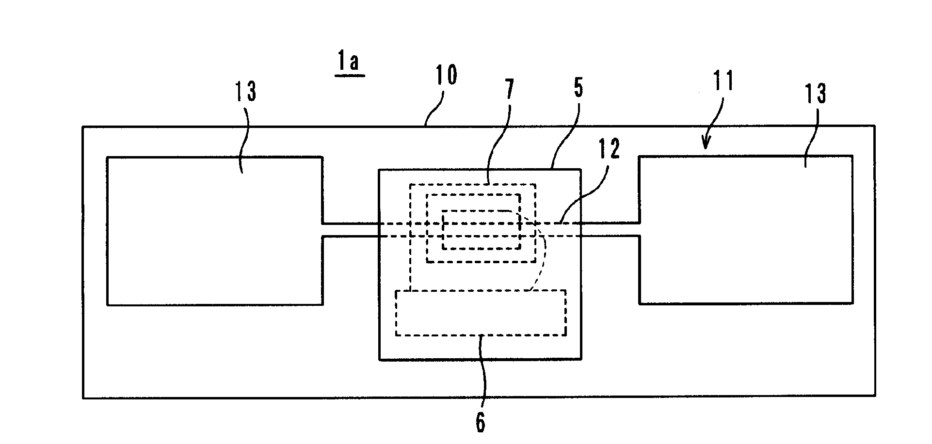
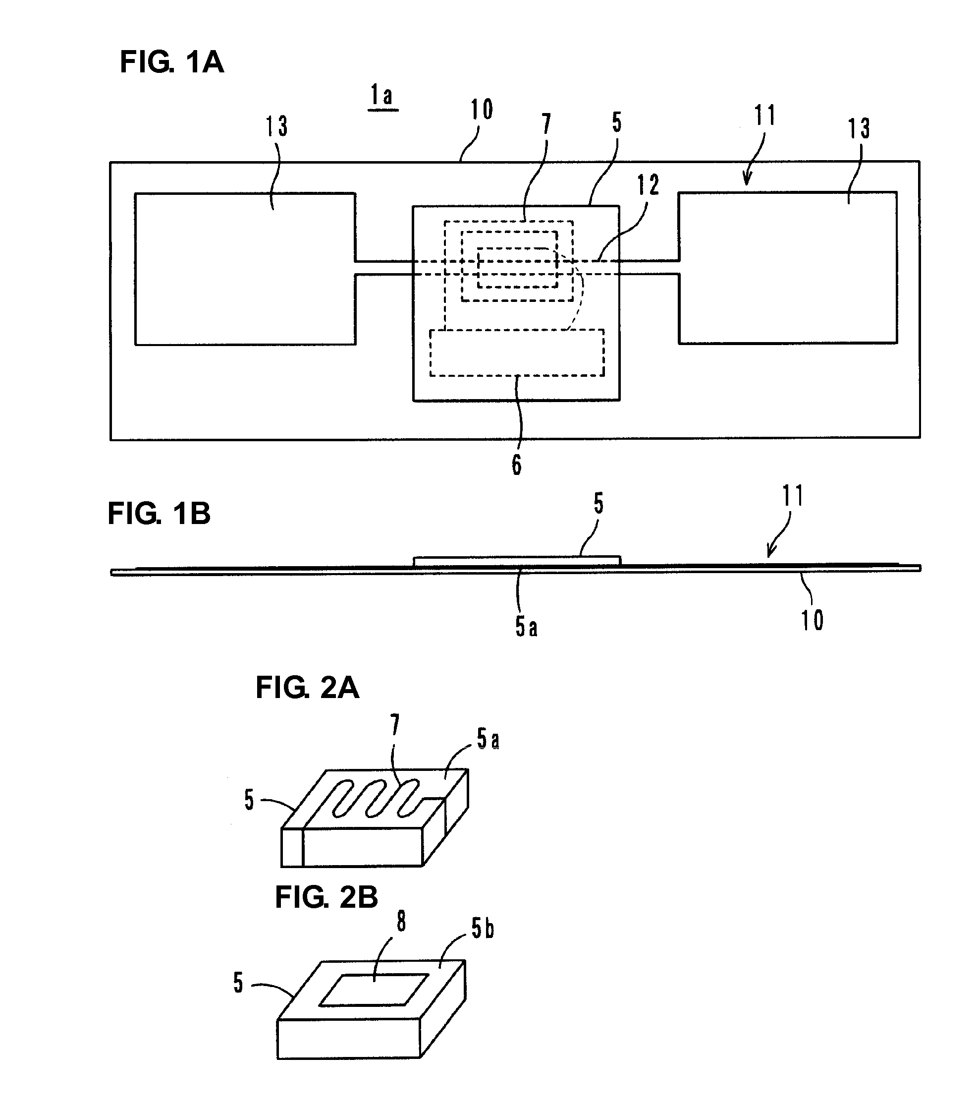
[0048]In a wireless IC device 1a according to a first preferred embodiment, as shown in FIGS. 1A and 1B, a radiation plate 11 is provided on a support film 10 and a wireless IC chip 5 is adhered by an adhesive, for example, on a power supply portion 12 on the radiation plate 11 over the support film 10. The radiation plate 11 is a two-surface-open type including the substantially linear power supply portion 12 and radiation portions 13 that are larger than the power supply portion 12. The radiation plate 11 is preferably made of a flexible metal thin film, such as an aluminum foil or a metal evaporated film, for example. The support film 10 is a flexible insulative film preferably made of, for example, polyethylene terephthalate (PET). The support film 10 may also be made of paper or synthetic paper.

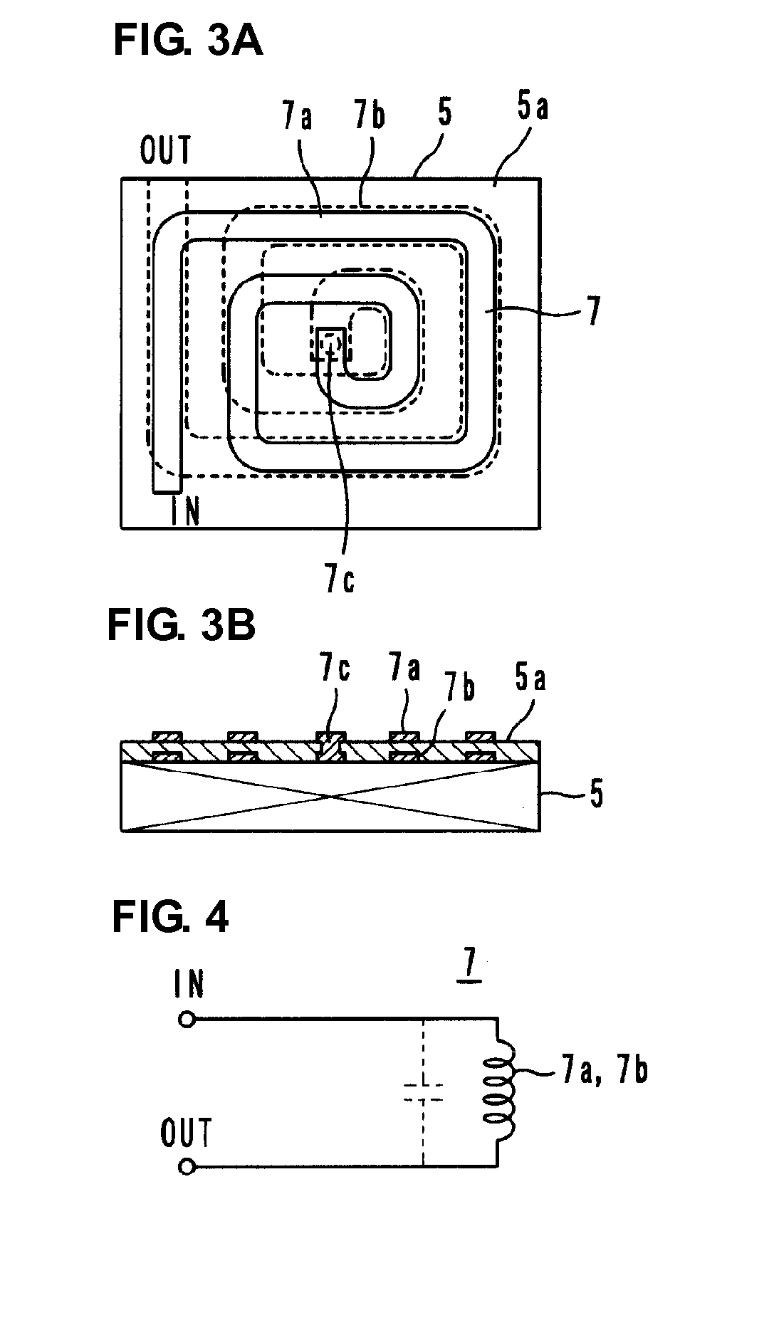
[0049]The wireless IC chip 5 includes a signal processing portion 6. A power supply circuit 7 defined by a coiled electrode pattern is arranged on a first principal surface 5a opposing t...

second preferred embodiment

[0060]In a wireless IC device 1b according to a second preferred embodiment of the present invention, as shown in FIG. 5, the radiation plate 11 preferably made of a metal thin film, such as an aluminum foil or a metal evaporated film, for example, is arranged on the support film 10. The radiation plate 11 includes the cruciform power supply portion 12 and relatively large radiation portions 13 that are connected to all of the ends of the power supply portion 12 and that extend in the x direction and the y direction. The wireless IC chip 5 is adhered by an adhesive, for example, on the support film 10 such that the center of the power supply circuit 7 substantially coincides with the cross-point of the power supply portion 12. Although the center of the power supply circuit 7 preferably substantially coincides with the cross-point of the power supply portion 12, the center of the power supply circuit 7 may be slightly shifted from the cross-point of the power supply portion 12.

[0061...

third preferred embodiment

[0062]In a wireless IC device 1c according to a third preferred embodiment of the present invention, as shown in FIG. 6, the power supply circuits 7 including two coiled electrode patterns are provided on the rear surface of the wireless IC chip 5 and the linear power supply portion 12 on the radiation plate 11 is arranged between the power supply circuits 7.

[0063]FIG. 7 shows a wireless IC device 1c′ according to a modification of the third preferred embodiment. In the wireless IC device 1c′, the power supply circuits 7 of the wireless IC chip 5 are defined by two meandering electrode patterns. The remaining arrangement is similar to that of the wireless IC device 1c. The horizontal meandering patterns may used or the vertical meander patterns may be used, for example.

[0064]The operational effects of the wireless IC device 1c and the wireless IC device 1c′ are similar to those in the first preferred embodiment described above. Specifically, a high-frequency signal (for example, a U...


PUM


Abstract

A wireless IC device includes a wireless IC chip having a power supply circuit including a resonant circuit having a predetermined resonant frequency and a radiation plate that externally radiates a transmission signal supplied from the power supply circuit and that supplies a reception signal externally transmitted to the power supply circuit. The radiation plate is connected to the power supply circuit via an electric field or the radiation plate is coupled to the power supply circuit via a magnetic field. The radiation plate is a two-surface-open type radiation plate including at least one radiation portion arranged to externally exchange a transmission-reception signal and a power supply portion arranged to exchange a transmission-reception signal with the power supply circuit.

Description

BACKGROUND OF THE INVENTION[0001]1. Field of the Invention[0002]The present invention relates to wireless integrated circuit (IC) devices and, more particularly, to a wireless IC device used in a Radio Frequency Identification (RFID) system.[0003]2. Description of the Related Art[0004]RFID systems have been developed as management systems for articles. In the RFID systems, readers-writers that generate induction fields communicate with IC tags (hereinafter referred to as wireless IC devices) that contain information regarding the articles by non-contact methods so as to transmit information. The wireless IC devices used in the RFID systems typically includes wire-wound coils that are formed on substrates on which wireless IC chips are mounted by etching or printing, for example.[0005]Japanese Unexamined Patent Application Publication No. 2000-276569 discloses a wireless IC device formed by rewiring an antenna coil on a wireless IC chip so as to reduce the size thereof. However, sinc...

Claims


Application Information

Patent Timeline
Patent Type & Authority Applications(United States)
IPC IPC(8): H04B7/00
CPCG06K19/07749G06K19/07786H01Q1/2208H01Q23/00H01Q9/28H01Q21/08H01Q21/24H01Q1/38
Inventor KATO, NOBORU
Owner MURATA MFG CO LTD
Why Eureka
Try Eureka