Method of forming contact plug in semiconductor device

a technology of contact plug and semiconductor device, which is applied in the manufacturing of semiconductor/solid-state devices, electrical equipment, basic electric elements, etc., can solve the problems of reducing the size unable to secure the unable to secure the bottom critical dimension of the contact hole, so as to improve the capability of contact gap filling

Inactive Publication Date: 2009-01-01
SK HYNIX INC
View PDF6 Cites 6 Cited by
  • Summary
  • Abstract
  • Description
  • Claims
  • Application Information

AI Technical Summary

Benefits of technology

[0007]The invention provides a method of forming a contact plug in a semiconductor device which can secure a bottom critical dimension of a contact hole and a distance

Problems solved by technology

However, as semiconductor devices have become more highly-integrated, the size of the contact hole has been reduced, and it has become difficult to secure a distance between the contact holes for insulating the contact holes.
As such, there is a problem in that, even though a space between top portions of the contact holes is secured due to

Method used


Image

  • Method of forming contact plug in semiconductor device
  • Method of forming contact plug in semiconductor device
  • Method of forming contact plug in semiconductor device

Examples


Embodiment Construction

[0014]Hereinafter, a preferred embodiment of the invention is explained in more detail with reference to the accompanying drawings. However, the embodiments of the invention may be modified variously and the scope of the invention should not be limited to the below embodiment. The description herein is provided for illustrating more completely to those skilled in the art.

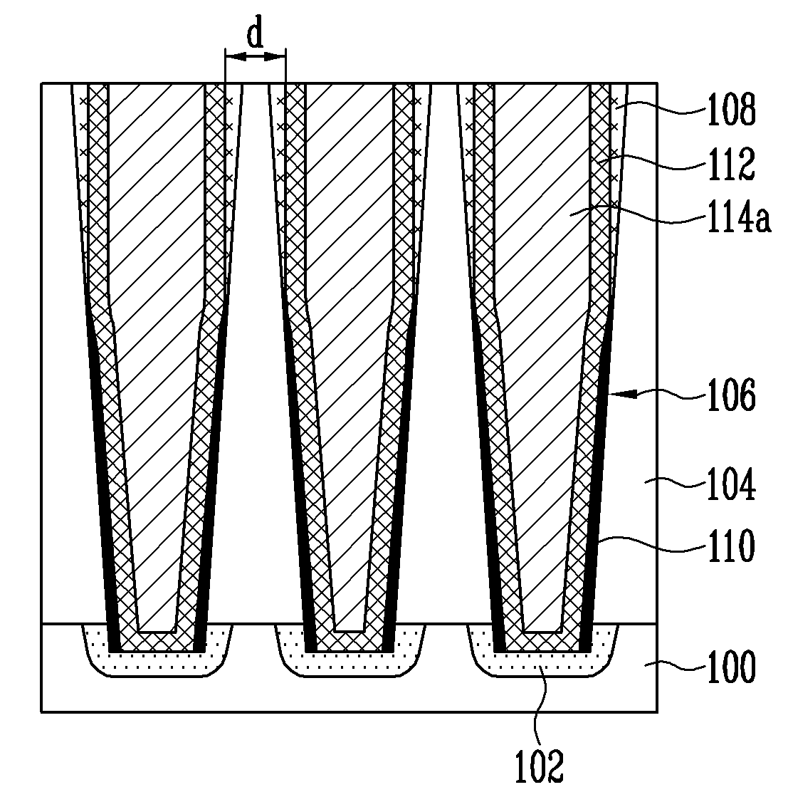
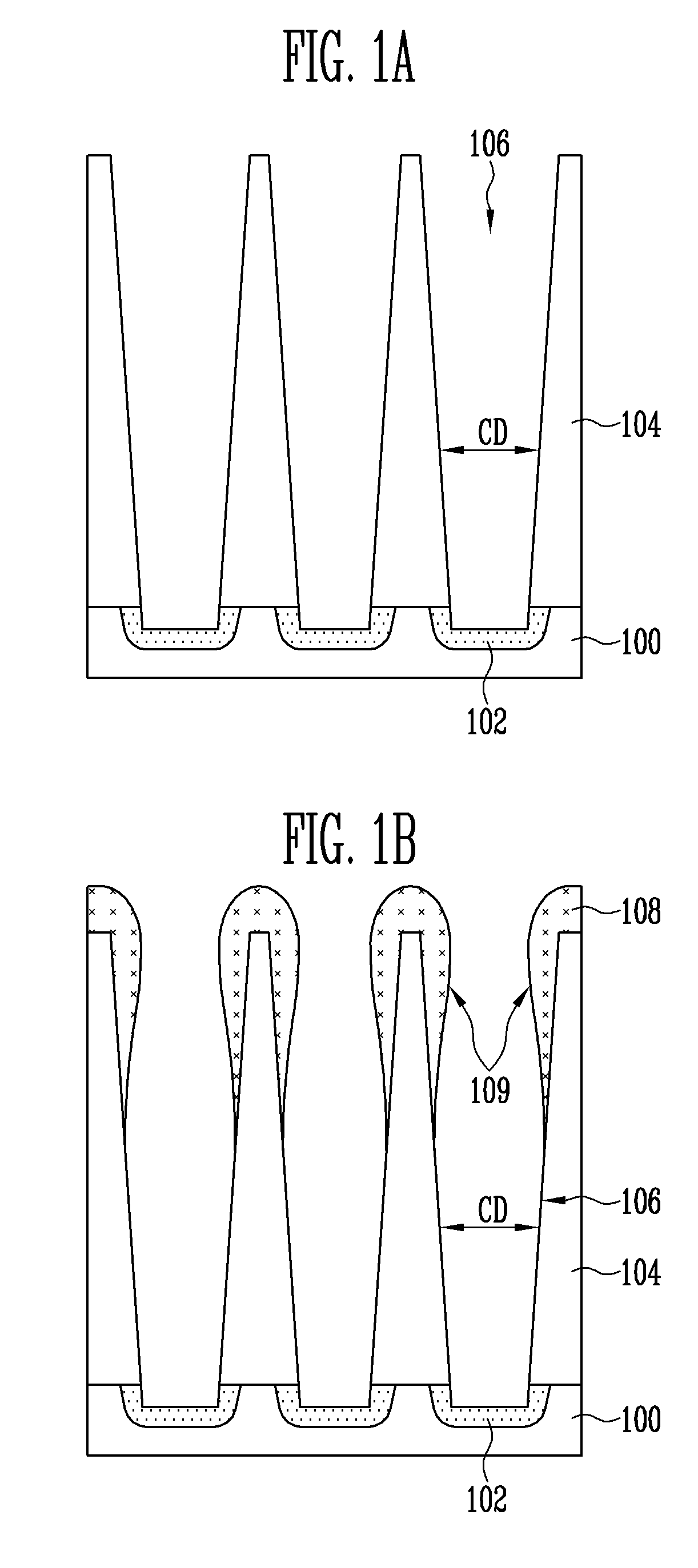
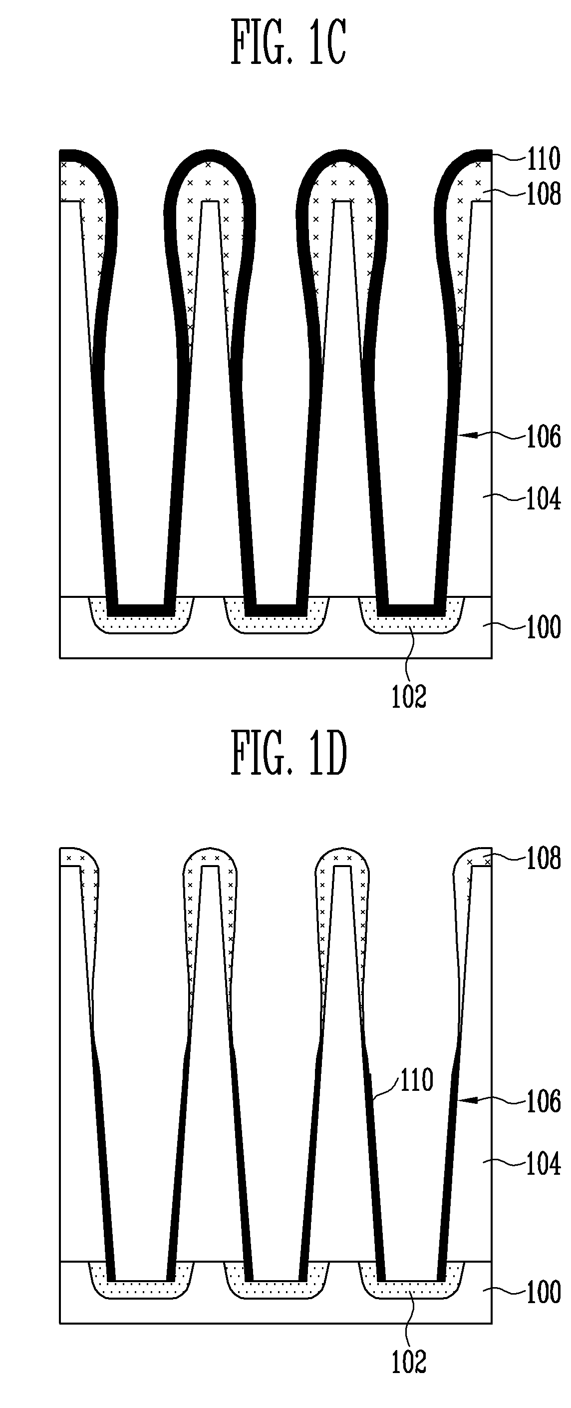
[0015]FIG. 1A to FIG. 1H are sectional views of a semiconductor device for illustrating a method of forming a contact plug in a semiconductor device according to one embodiment of the invention.

[0016]Referring to FIG. 1A, an interlayer insulating layer 104 is formed on a semiconductor substrate 100 on which junction areas 102 are formed. Any suitable oxidized material can be used for forming the interlayer insulating layer 104. For example, any of SOG (spin on glass), BPSG (boron-phosphorus silicate glass), PETEOS (plasma enhanced tetra Ethyl ortho silicate), USG (undoped silicate glass), PSG (phosphorus silicate gl...


PUM


Abstract

A method of forming a contact plug in a semiconductor device comprising etching an interlayer insulating layer to form a patterned interlayer insulating layer having contact holes such that a distance between upper portions of the contact holes is minimized; forming a first insulating layer including a overhang portion for wrapping an upper portion of the patterned interlayer insulating layer; forming a liner-shaped second insulating layer on the patterned interlayer insulating layer including the first insulating layer, the second insulating layer being formed from material having a selectivity which differs from that of the first insulating layer; and at least partially removing the second insulating layer to increase a bottom critical dimension of the contact hole and removing the overhang portion of the first insulating layer. The invention can secure the bottom critical dimension of the contact hole as well as a distance between the upper portions of the contact holes when the contact plug is formed in a trench in a subsequent process so that the subsequent process margin can be secured. Also, the invention can inhibit an overhang or seam from being formed on the contact plug to enhance contact gap-fill capability and improve contact resistance.

Description

CROSS-REFERENCE TO RELATED APPLICATION[0001]The priority of Korean Patent Application No. 2007-64306, filed on Jun. 28, 2007, the contents of which are incorporated herein by reference in its entirety, is claimed.BACKGROUND OF THE INVENTION[0002]The invention relates to a method of forming a contact plug in a semiconductor device and, more particularly, relates to a method of forming a contact plug in a semiconductor device which can secure a bottom critical dimension of a contact hole as well as a distance between upper portions of contact holes to secure a subsequent process margin.[0003]In a semiconductor device provided with multilayered metal wires, a contact plug is formed by filling a contact hole for electrically connecting an upper element to a lower element. For forming the contact hole in the semiconductor device, an accurate and strict mask alignment is required in the manufacturing process.[0004]A conventional process for forming a contact plug in a semiconductor device...

Claims


Application Information

Patent Timeline
IPC IPC(8): H01L21/44
CPCH01L21/31116H01L21/76832H01L21/76816H01L21/76814H01L21/28
Inventor KIM, EUN SOOKIM, JUNG GEUNHONG, SEUNG HEE
Owner SK HYNIX INC
Why Eureka
Try Eureka