Accurate Parasitic Capacitance Extraction for Ultra Large Scale Integrated Circuits

a parasitic capacitance and ultra-large-scale technology, applied in semiconductor/solid-state device testing/measurement, semiconductor/solid-state device details, instruments, etc., can solve problems such as undesired long signal delay, detrimental effect, and existing extraction methodology problems, and achieve the effect of improving accuracy

Inactive Publication Date: 2009-01-01
TAIWAN SEMICON MFG CO LTD
View PDF38 Cites 24 Cited by
  • Summary
  • Abstract
  • Description
  • Claims
  • Application Information

AI Technical Summary

Benefits of technology

[0018]An advantage of a preferred embodiment of the present invention is that parasitic capacitance associated with actual contact / via shapes and size variations are extracted with substantially improved accuracy. This is achieved without overhauls on existing “polygon-based” full-chip extraction tools.
[0019]A further advantage of a preferred embodiment of the present invention is that once the accuracy of an “Effective Contact Width” and “Effective via Width” table in preferred embodiments are verified passing a quality assurance (QA) criteria by a silicon vendor, the technology file derived thereupon can be released to any design teams. IC designers do not need to change an established extraction flow.

Problems solved by technology

If the parasitic capacitance and resistance causes undesirable performance, the integrated circuit layout is typically changed through one or more design optimization cycles.
It is known that the parasitic capacitance and resistance can cause various detrimental effects in a designed IC, such as undesired long signal delays on the nets.
The existing extraction methodology is problematic in contact / via parasitic capacitance extraction.
The lack of extraction accuracy on contact and via capacitance may cause large discrepancies between simulated results and actual circuit performance.
As a result, the simulated results can be overly pessimistic with a margin of over 10%.

Method used


Image

  • Accurate Parasitic Capacitance Extraction for Ultra Large Scale Integrated Circuits
  • Accurate Parasitic Capacitance Extraction for Ultra Large Scale Integrated Circuits
  • Accurate Parasitic Capacitance Extraction for Ultra Large Scale Integrated Circuits

Examples


Embodiment Construction

[0033]The making and using of the presently preferred embodiments are discussed in detail below. It should be appreciated, however, that the present invention provides many applicable inventive concepts that can be embodied in a wide variety of specific contexts. The specific embodiments discussed are merely illustrative of specific ways to make and use the invention, and do not limit the scope of the invention.

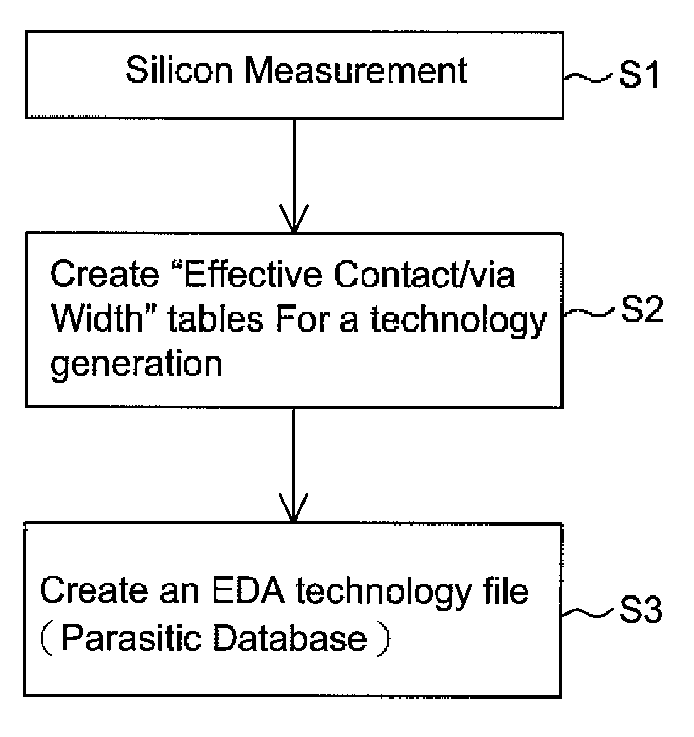
[0034]The present invention will be described with respect to preferred embodiments in a specific context, namely a parasitic capacitance extraction method that takes account of the actual contact / via shapes and size variations. A common feature of the various embodiments is to replace the ideal, square-shaped contact / via configuration, which is used to “extract” the full-chip parasitic capacitance, with an indexed “Effective Contact Width” table and “Effective via Width” table, respectively. Each element of such a table represents an ideal, squared-shaped contact / via configu...


PUM


Abstract

A system and method for extracting the parasitic contact / via capacitance in an integrated circuit are provided. Parasitic extraction using this system can lead to an improved accuracy on contact / via parasitic capacitance extraction by taking into account of the actual contact / via shape and size variation. The common feature of the various embodiments includes the step of generating a technology file, in which the contact / via capacitance in the capacitance table is derived from an effective contact / via width table. Each element of the effective contact / via width table is calibrated to have a parasitic capacitance matching to that of an actual contact / via configuration occurring in an IC.

Description

[0001]This application claims the benefit of U.S. provisional application No. 60 / 947,269, filed on Jun. 29, 2007, entitled “Method And System to Enable Design Optimization of Via and Contact,” which application is hereby incorporated herein by reference.CROSS-REFERENCE TO RELATED APPLICATIONS[0002]This application relates to the following co-pending and commonly assigned patent application Ser. No. ______, filed ______, entitled “Accurate Capacitance Measurement for Ultra Large Scale Integrated Circuits” (TSM07-0335), which application is hereby incorporated herein by reference.TECHNICAL FIELD[0003]The present invention relates generally to integrated circuit design, and more particularly to extracting parasitic capacitance in a semiconductor device.BACKGROUND[0004]Integrated circuits (“ICs”) vary in complexity from, for example, an analog circuit comprising only a few basic electronic components, such as transistors and diodes, to a complex digital system including hundreds of mill...

Claims


Application Information

Patent Timeline
Patent Type & Authority Applications(United States)
IPC IPC(8): G06F17/50
CPCG01R31/2853G01R31/2884H01L22/34H01L2924/0002H01L2924/00
Inventor SU, KE-YINGHO, CHIA-MINGCHANG, GWAN SINCHEN, CHIEN-WEN
Owner TAIWAN SEMICON MFG CO LTD
Why Eureka
Try Eureka