Oxide semiconductor, thin film transistor including the same and method of manufacturing a thin film transistor

a thin film transistor and semiconductor technology, applied in the direction of semiconductor devices, basic electric elements, electrical equipment, etc., can solve the problems of poor uniformity, limited use of p-si tfts, and multiple complicated and expensive processes, and achieve the effect of increasing the electrical properties of the thin film transistor

Inactive Publication Date: 2009-01-08
SAMSUNG ELECTRONICS CO LTD
View PDF2 Cites 272 Cited by
  • Summary
  • Abstract
  • Description
  • Claims
  • Application Information

AI Technical Summary

Benefits of technology

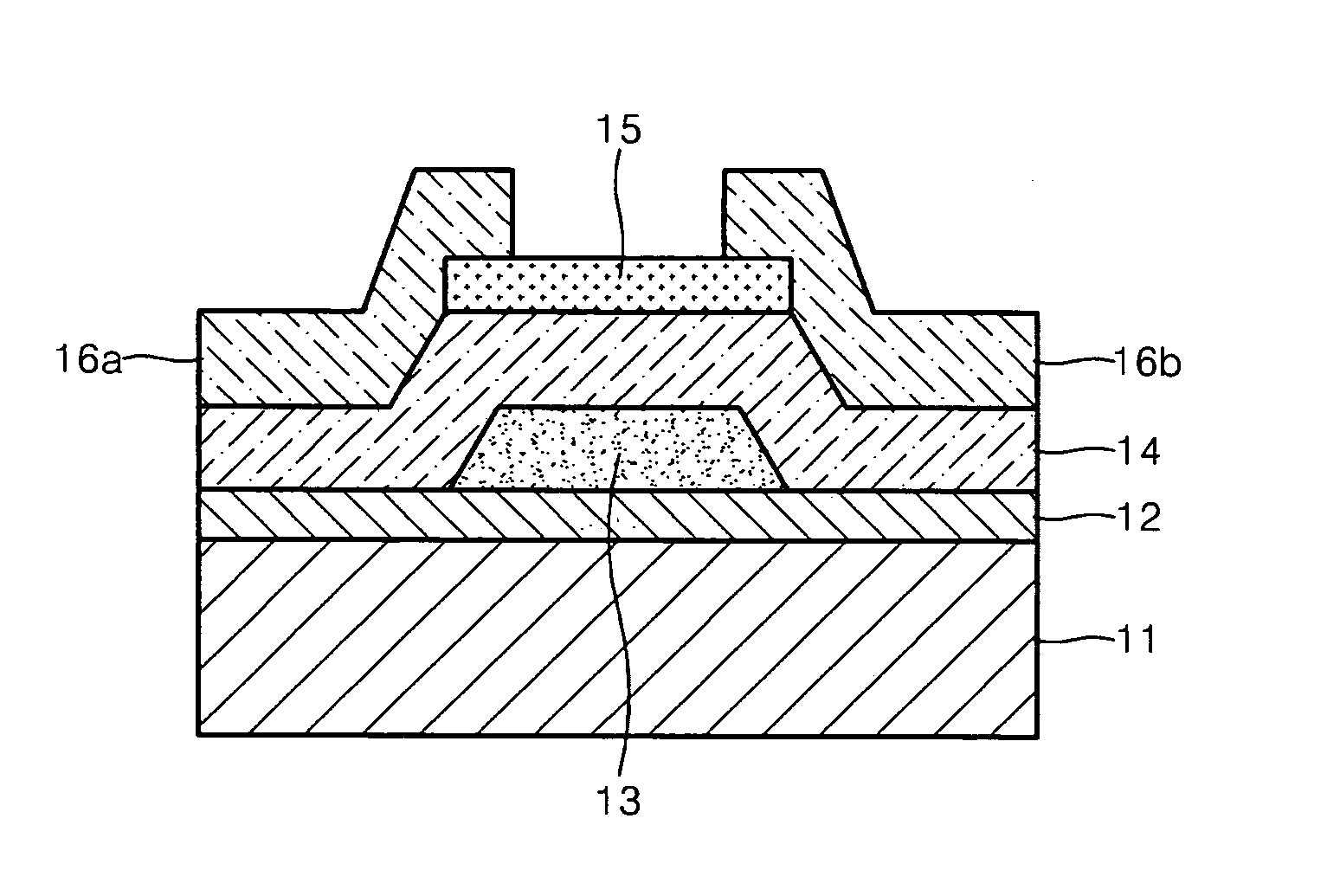
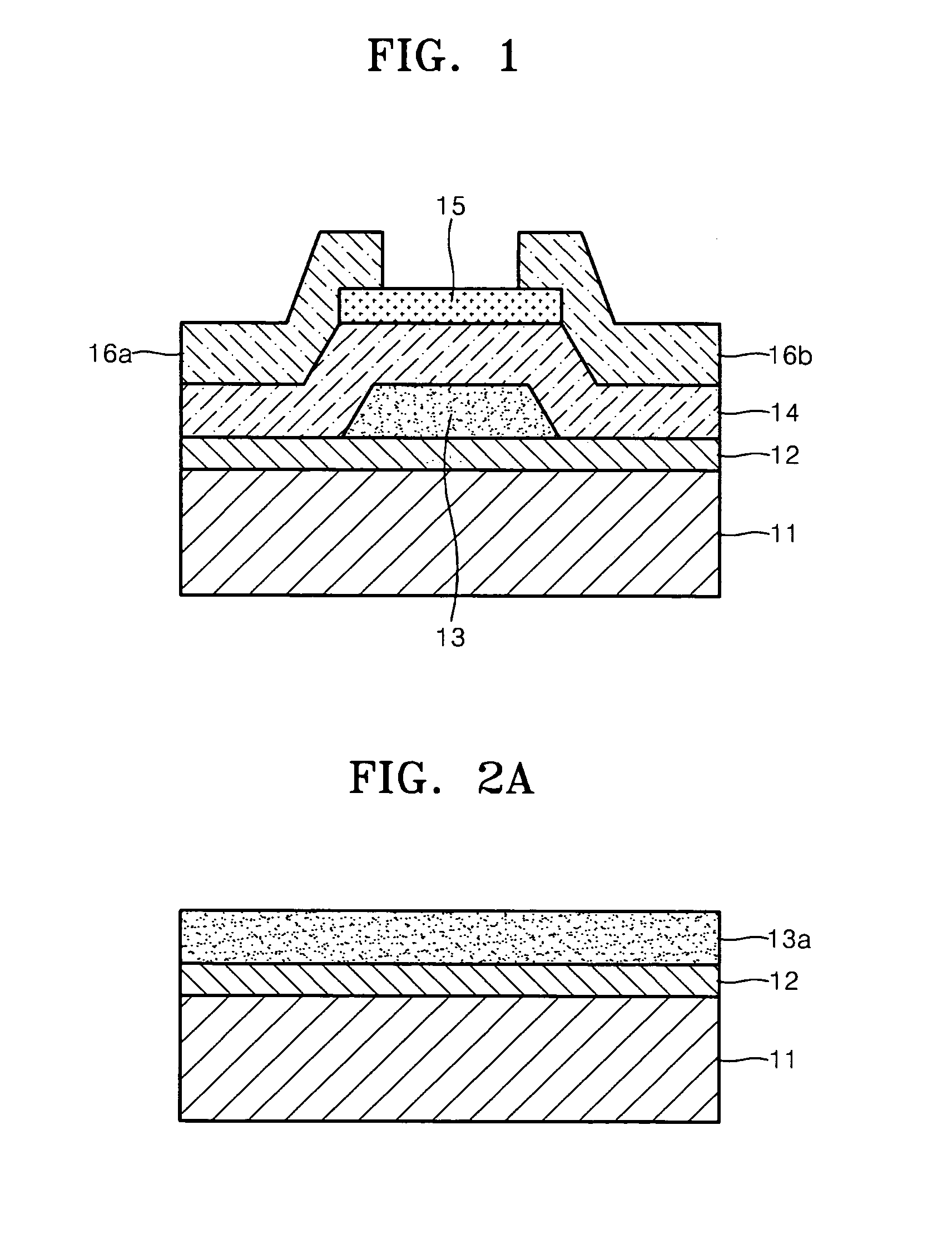
[0014]Other example embodiments provide a thin film transistor including a channel formed of the oxide semiconductor that increases electrical properties of the thin film transistor.

Problems solved by technology

Manufacturing p-Si TFTs involves performing several complicated and expensive processes.
Because p-Si TFTs are less cost-effective than conventional a-Si TFTs, the use of p-Si TFTs may be limited.
Because manufacturing a large-sized substrate having a side length greater than 1 m has not been realized yet due to technical problems (e.g., manufacturing equipments limits, poor uniformity, etc.), it is cumbersome to use p-Si TFTs in displays (including televisions and computer monitors) and other display products.

Method used


Image

  • Oxide semiconductor, thin film transistor including the same and method of manufacturing a thin film transistor
  • Oxide semiconductor, thin film transistor including the same and method of manufacturing a thin film transistor
  • Oxide semiconductor, thin film transistor including the same and method of manufacturing a thin film transistor

Examples


Embodiment Construction

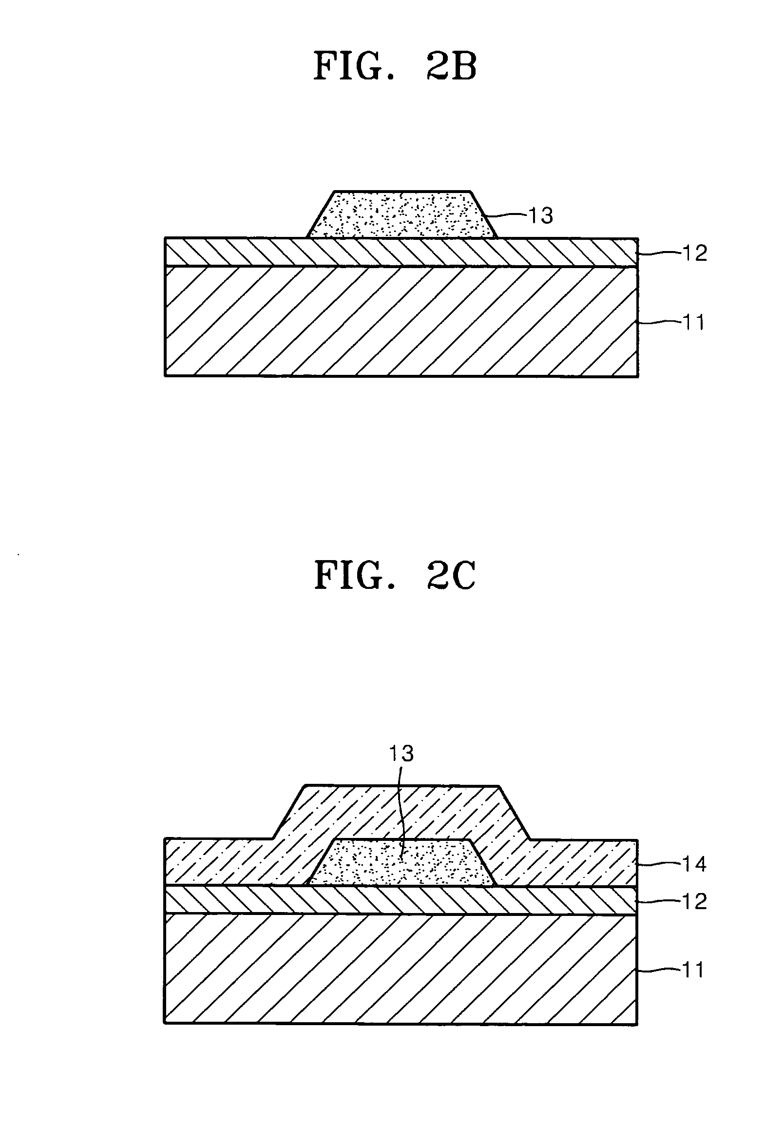
[0035]Reference will now be made in detail to example embodiments, examples of which are illustrated in the accompanying drawings. However, example embodiments are not limited to the embodiments illustrated hereinafter, and the embodiments herein are rather introduced to provide easy and complete understanding of the scope and spirit of example embodiments. In the drawings, the thicknesses of layers and regions are exaggerated for clarity.

[0036]It will be understood that when an element or layer is referred to as being “on,”“connected to” or “coupled to” another element or layer, it may be directly on, connected or coupled to the other element or layer or intervening elements or layers may be present. In contrast, when an element is referred to as being “directly on,”“directly connected to” or “directly coupled to” another element or layer, there are no intervening elements or layers present. Like reference numerals refer to like elements throughout. As used herein, the term “and / or...


PUM

PropertyMeasurementUnit
thicknessaaaaaaaaaa
temperatureaaaaaaaaaa
side lengthaaaaaaaaaa

Abstract

Example embodiments relate to an oxide semiconductor including zinc oxide (ZnO), a thin film transistor including a channel formed of the oxide semiconductor and a method of manufacturing the thin film transistor. The oxide semiconductor may include a GaxInyZnz oxide and at least one material selected from the group consisting of a 4A group element, a 4A group oxide, a rare earth element and combinations thereof.

Description

PRIORITY STATEMENT[0001]This application claims the benefit of priority under 35 USC §119 from Korean Patent Application No. 10-2007-0067131, filed on Jul. 4, 2007 in the Korean Intellectual Property Office (KIPO), the entire contents of which are herein incorporated by reference.BACKGROUND[0002]1. Field[0003]Example embodiments relate to an oxide semiconductor and a thin film transistor including the same. Other example embodiments relate to an oxide semiconductor including zinc oxide (ZnO), a thin film transistor including a channel formed of the oxide semiconductor and a method of manufacturing the thin film transistor.[0004]2. Description of the Related Art[0005]A thin film transistor may be used in a variety of fields. Thin film transistors may be used as switching devices and driving devices. Thin film transistors may be used as switches to select a cross-point memory.[0006]An amorphous silicon thin film transistor (a-Si TFT) may be used as a driving device and a switching dev...

Claims


Application Information

Patent Timeline
Patent Type & Authority Applications(United States)
IPC IPC(8): H01L29/12H01L21/336
CPCH01L29/7869H01L29/26
Inventor KANG, DONG-HUNSONG, I-HUNPARK, YOUNG-SOOKIM, CHANG-JUNGLEE, EUN-HALEE, JAE-CHEOL
Owner SAMSUNG ELECTRONICS CO LTD
Why Eureka
Try Eureka