Clock generation circuit, recording device and clock generation method

a clock generation circuit and recording device technology, applied in the direction of generating/distributing signals, recording signal processing, instruments, etc., can solve the problems of signal sometimes temporarily lost, signal strength reduced, recording is not in the correct format, etc., to and reduce the time difference between the input synchronizing signal and the output synchronizing signal.

Inactive Publication Date: 2009-01-08
SONY CORP
View PDF6 Cites 2 Cited by
  • Summary
  • Abstract
  • Description
  • Claims
  • Application Information

AI Technical Summary

Benefits of technology

[0019]According to another embodiment of the present invention, there is provided a recording device that includes: a PLL circuit that multiplies an input signal of a specific frequency read from a recording medium by a specific multiplication factor and generates a recording clock signal that is used to record recording data onto the recording medium; and a correction circuit that changes the multiplication factor of the PLL circuit. The correction circuit changes the PLL circuit multiplication factor from the specific multiplication factor to a multiplication factor that is established increasing or decreasing the specific multiplication factor, the change being performed only over a correction interval for each correction cycle, the correction cycle being longer than one cycle of the input signal, and the change being performed such that a time difference between an input synchronizing signal that is synchronized with the input signal and a recording synchronizing signal that is repeatedly attached to the recording data at a specific interval is reduced, and the PLL circuit multiplies the input signal by the changed multiplication factor during the correction interval. With this configuration, the time difference between the input synchronizing signal and the output synchronizing signal can be reduced.
[0020]According to another embodiment of the present invention, there is provided a clock generation method that includes the steps of: changing a multiplication factor that multiplies an input signal of a specific frequency from a specific multiplication factor to a multiplication factor that is set by increasing or decreasing the specific multiplication factor, the change being performed only during a correction interval for each correction cycle, the correction cycle being longer than one cycle of the input signal, and the change being performed such that a time difference between an input synchronizing signal that is synchronized with the input signal and an output synchronizing signal that is synchronized with an output clock signal is reduced; and generating the output clock signal by multiplying the input signal using the changed multiplication factor during the correction interval. With this configuration, the time difference between the input synchronizing signal and the output synchronizing signal can be reduced.
[0021]According to the embodiments of the present invention described above, deviation in the output clock signal occurring due to the lost of the input signal can be appropriately corrected and an output clock signal that is synchronized with the input signal can be generated.

Problems solved by technology

However, the strength of the wobble signal read by the recording device is sometimes reduced by a manufacturing error in the recording medium, or by contamination of or a flaw in the recording medium, and the signal is sometimes temporarily lost.
When positional deviation occurs, even if writing of the recording data is continued and recording is completed, the recording is not in the correct format, and sometimes the data cannot be read out appropriately.

Method used


Image

  • Clock generation circuit, recording device and clock generation method
  • Clock generation circuit, recording device and clock generation method
  • Clock generation circuit, recording device and clock generation method

Examples


Embodiment Construction

)

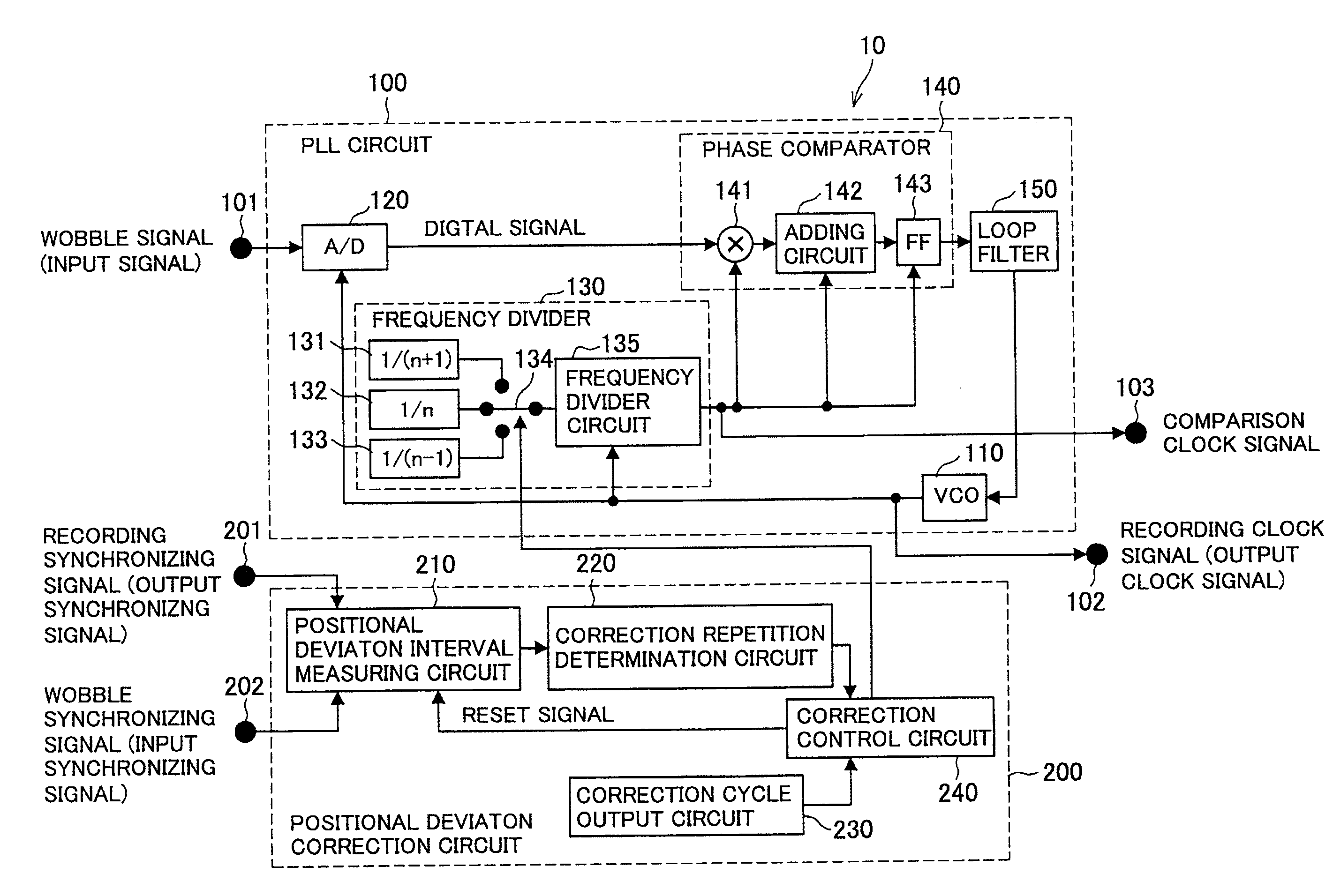
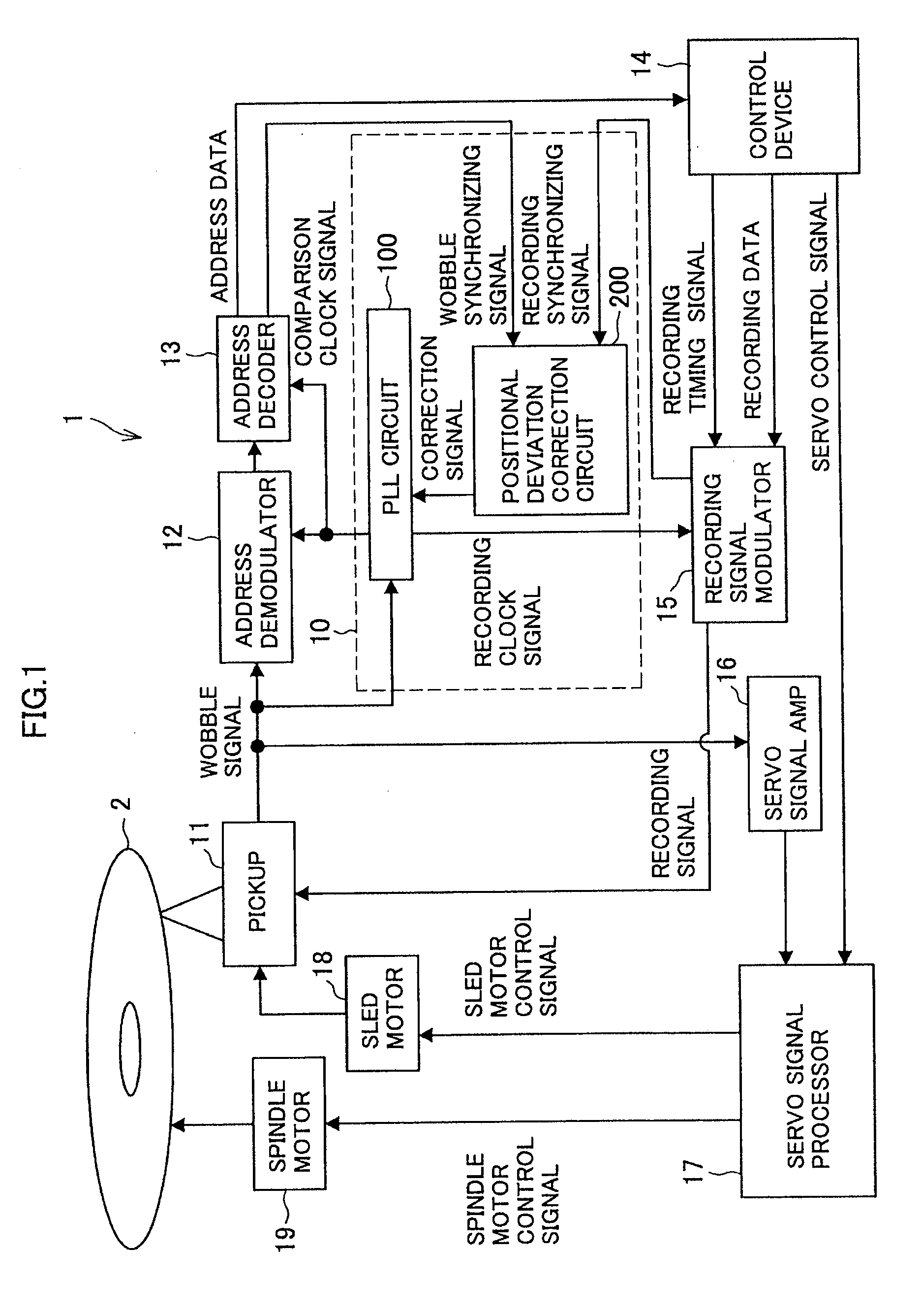
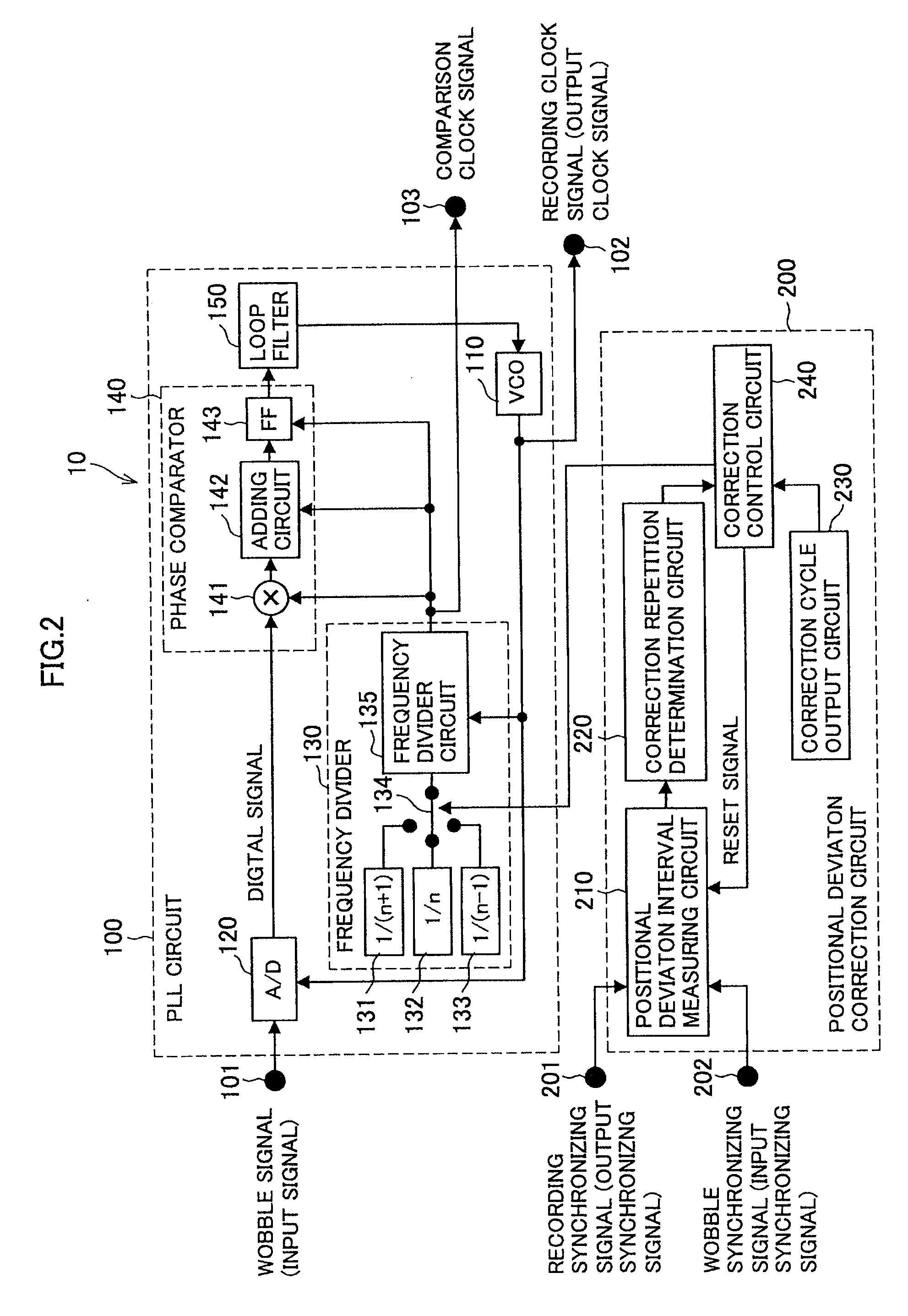
[0033]Hereinafter, preferred embodiments of the present invention will be described in detail with reference to the appended drawings. Note that, in this specification and the appended drawings, structural elements that have substantially the same function and structure are denoted with the same reference numerals, and repeated explanation of these structural elements is omitted.

[0034]Clock Generation Circuits According to Related Technology

[0035]Before explaining the embodiments of the present invention, a clock generation circuit according to related technology will be explained with reference to FIG. 9. FIG. 9 is a block diagram showing the structure of a clock generation circuit according to related technology.

[0036]As shown in FIG. 9, a clock generation circuit 300 according to related technology is formed of a PLL circuit that receives an analog input signal from an input terminal 301, and outputs a recording clock signal from an output terminal 302, the recording clock signa...


PUM


Abstract

A clock generation circuit is provided that multiplies an input signal of a specific frequency by a specific multiplication factor and generates an output clock signal. The clock generation circuit includes a PLL circuit that multiplies the input signal and generates the output clock signal, and a correction circuit that changes the multiplication factor of the PLL circuit. The correction circuit changes the PLL circuit multiplication factor by increasing or decreasing the specific multiplication factor, the change being performed only during a correction interval for each correction cycle, the correction cycle being longer than one cycle of the input signal, and being performed such that a time difference between an input synchronizing signal synchronized with the input signal and an output synchronizing signal synchronized with the output clock signal is reduced. The PLL circuit multiplies the input signal by the changed multiplication factor during the correction interval.

Description

CROSS REFERENCES TO RELATED APPLICATION(S)[0001]The present invention contains subject matter related to Japanese Patent Application JP 2007-174361 filed in the Japan Patent Office on Jul. 2, 2007, the entire contents of which being incorporated herein by reference.BACKGROUND OF THE INVENTION[0002]1. Field of the Invention[0003]The present invention relates to a clock generation circuit, a recording device and a clock generation method.[0004]2. Description of the Related Art[0005]In recent years, recording media such as optical disks that are recordable as well as allowing playback, have grooves formed in advance on the recording surface, and so-called wobble modulation is performed on these grooves to record address data (position data). When recording specific data to be recorded on a recording medium, a recording device extracts the address data as an electric signal (known as a wobble signal), multiplies the signal using a phase-lock loop (PLL) circuit and generates a write cloc...

Claims


Application Information

Patent Timeline
Patent Type & Authority Applications(United States)
IPC IPC(8): H03L7/06
CPCG11B20/10222G11B2020/1239G11B20/1403G11B20/10425G11B20/14G11B20/10H03L7/08
Inventor SANO, TATSUSHI
Owner SONY CORP
Why Eureka
Try Eureka