Clock generating apparatus

a clock generator and clock technology, applied in the direction of generating/distributing signals, instruments, pulse techniques, etc., can solve the problems of high cost of a very small interval clock generator and difficulty in transmitting multi-phase clock signals

Inactive Publication Date: 2009-01-08
SAMSUNG ELECTRONICS CO LTD
View PDF6 Cites 19 Cited by
  • Summary
  • Abstract
  • Description
  • Claims
  • Application Information

AI Technical Summary

Benefits of technology

[0026]The controllable delay line may be connected between an output for the first internal clock signal of the clock generator and an input of the clock generator to form a feedback path. The controllable delay line may be activated in a bit error rate test mode set by a user, and the control signal may be a signal applied by a user in the bit error rate test mode. Thus, the present invention may provide a clock generator capable of performing a bit error rate test.

Problems solved by technology

However, for the time sweep of the clock signal, the ATE device having a very small interval has high costs, and it is difficult to transmit multi-phase clock signals.

Method used


Image

  • Clock generating apparatus
  • Clock generating apparatus
  • Clock generating apparatus

Examples


Embodiment Construction

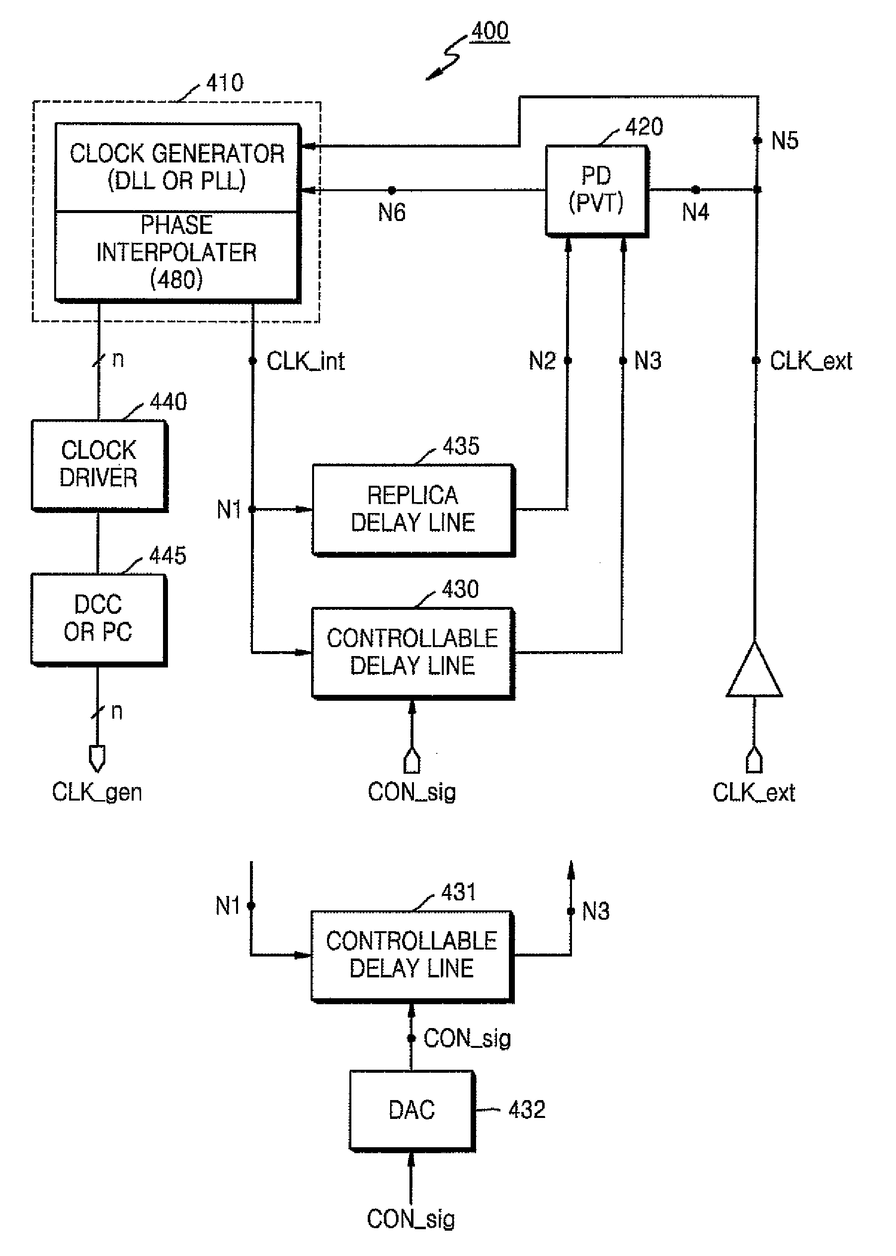
[0046]The present invention will now be described more fully with reference to the accompanying drawings, in which exemplary embodiments of the invention are shown. The invention, however, may be embodied in various different forms, and should not be construed as being limited only to the illustrated embodiments. Rather, these embodiments are provided as examples, to convey the concept of the invention to one skilled in the art. Accordingly, known processes, elements, and techniques are not described with respect to some of the embodiments of the present invention. Throughout the drawings and written description, like reference numerals will be used to refer to like or similar elements.

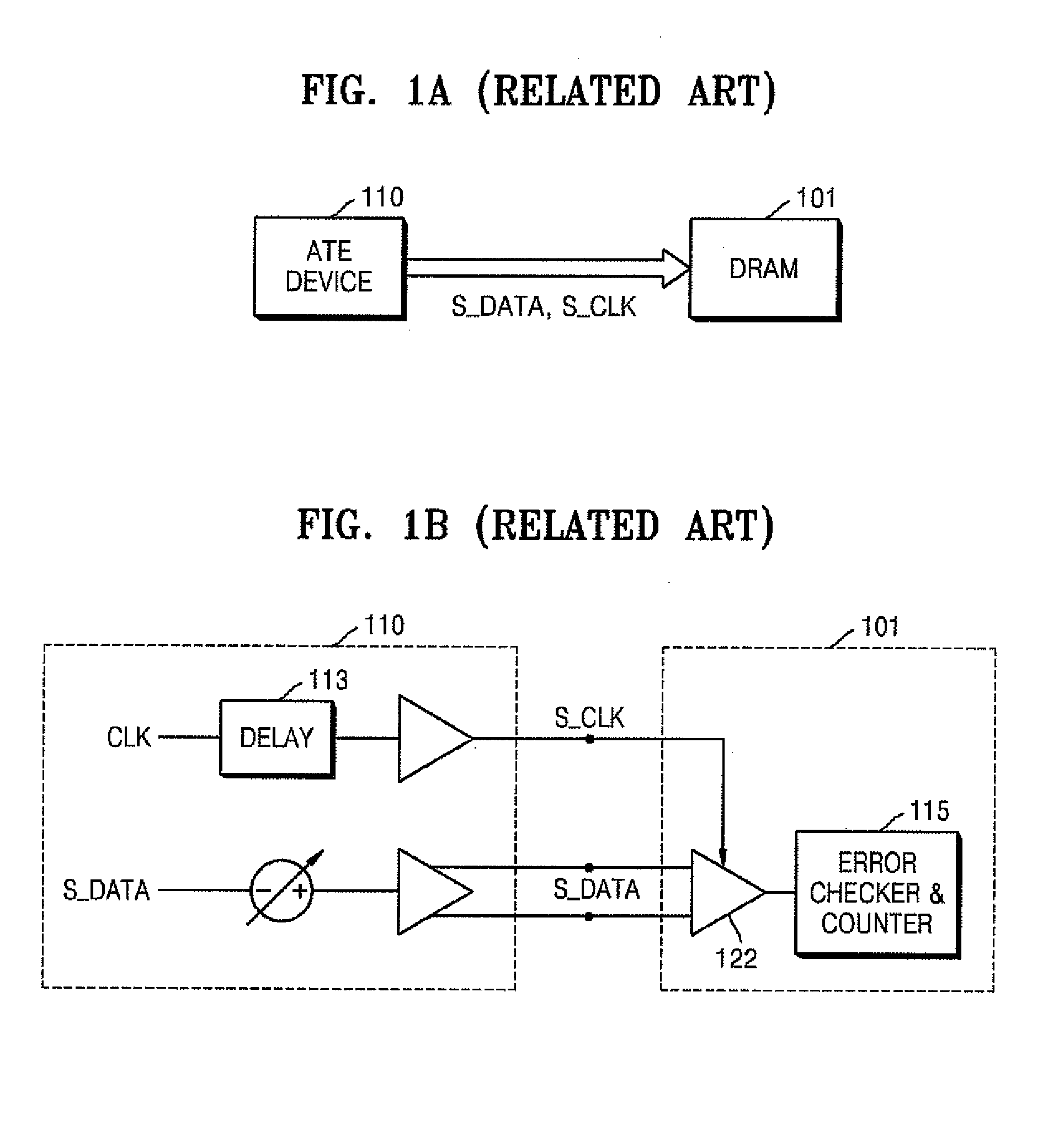
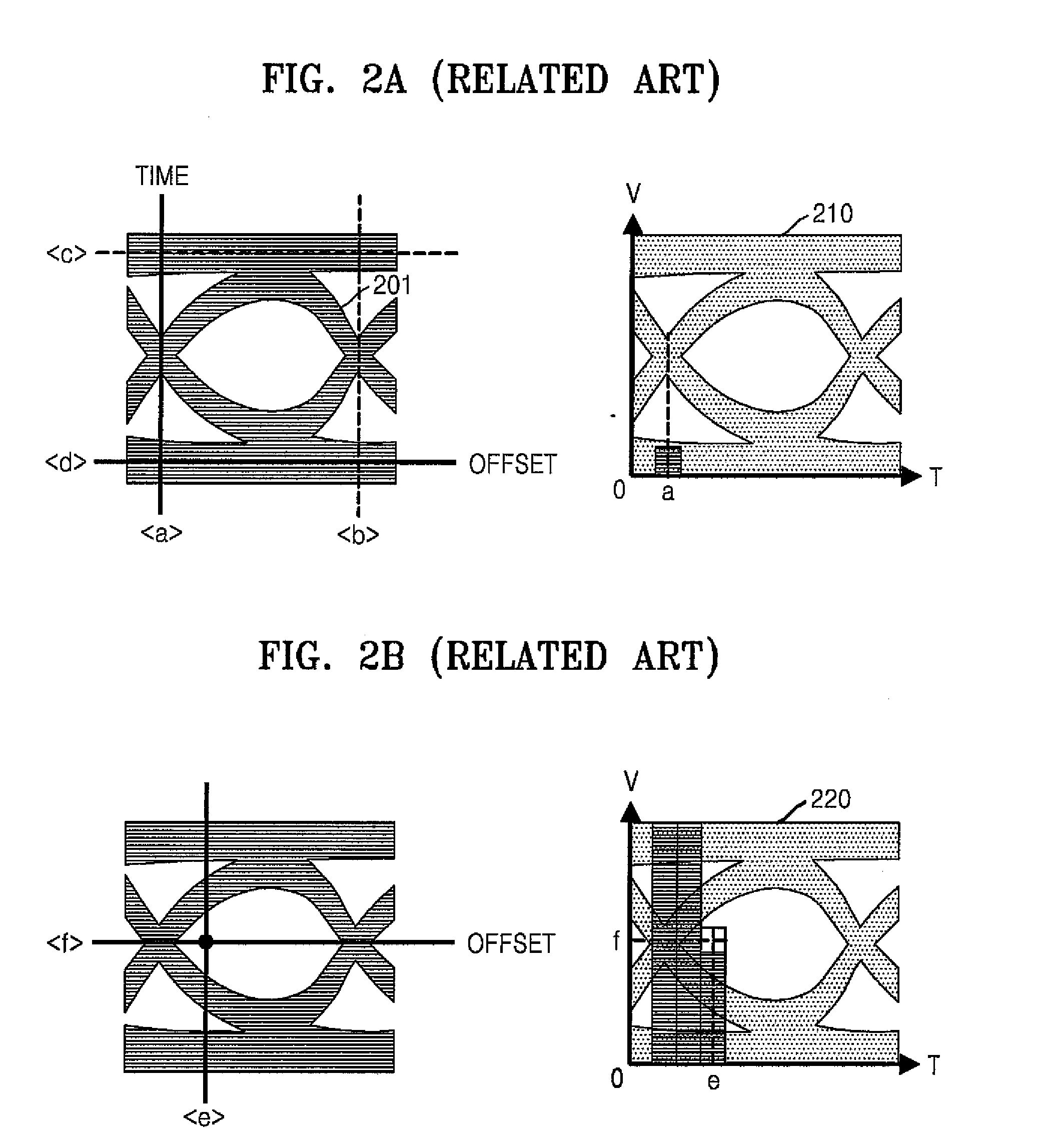
[0047]Densities and operating speeds of semiconductor devices have increased. A single data rate (SDR) synchronous dynamic random access memory (SDRAM) outputs 1-bit data per clock cycle, and a double data rate (DDR) SDRAM outputs 2-bit data per clock period. However, for high-speed signal processing ...


PUM


Abstract

A clock generating apparatus includes a clock generator and a controllable delay line. The clock generator receives an external clock signal and generates multiple clock signals having different phases by delaying the external clock signal. The controllable delay line receives one of the multiple clock signals as a first clock signal and delays the first clock signal by a first interval in response to an externally applied control signal. The delayed first clock signal is input to the clock generator.

Description

CROSS-REFERENCE TO RELATED PATENT APPLICATION[0001]A claim of priority is made to Korean Patent Application No. 10-2007-0066167, filed on Jul. 2, 2007, the subject matter of which is hereby incorporated by reference.BACKGROUND OF THE INVENTION[0002]1. Field of the Invention[0003]The present invention relates to a clock generator, and more particularly, to a clock generator for generating multiple clock signals having different phases.[0004]2. Description of the Related Art[0005]In order to test the reliability of a semiconductor device, a bit error rate (BER) is measured. For example, a dynamic random access memory (DRAM) restores a signal received from an external device (a measuring device of a memory controller) and transmits the restored signal back to the measuring device, or operations of an interface circuit between a transmitter and a receiver are verified by decision in a DRAM chip. As a method of testing the bit error rate, the DRAM receives and outputs data applied from t...

Claims


Application Information

Patent Timeline
Patent Type & Authority Applications(United States)
IPC IPC(8): H03K3/00
CPCG06F1/08H03K5/133H03L7/0812H03K2005/00052H03K2005/00208H03K5/15026H03L7/0816G11C11/4076G11C11/407G11C29/00
Inventor JANG, YOUNG-CHAN
Owner SAMSUNG ELECTRONICS CO LTD
Why Eureka
Try Eureka