Solid-state imaging device and imaging apparatus

a technology of imaging device and imaging apparatus, which is applied in the direction of color television details, television system details, television systems, etc., can solve the problems of causing harm by performing such differential processing, and achieve the effect of affecting harm and being easily affected

Active Publication Date: 2009-01-08
SONY CORP
View PDF4 Cites 46 Cited by
  • Summary
  • Abstract
  • Description
  • Claims
  • Application Information

AI Technical Summary

Benefits of technology

[0019]The solid-state imaging device may be formed as one chip or may be a module-like form having an imaging function formed by collectively packaging an imaging unit and a signal processing unit or an optical system. The present invention is applicable not only to the solid-state imaging device but also to an imaging apparatus. When the present invention is applied to the imaging apparatus, the imaging apparatus obtains an effect same as that of the solid-state imaging device. The imaging apparatus refers to a camera or a portable apparatus having an imaging function. “Imaging” includes not only capturing of an image during normal camera photographing but also fingerprint detection and the like in a broader sense.
[0020]According to the e

Problems solved by technology

However, it has been found that, under a certain imaging condition, h

Method used


Image

  • Solid-state imaging device and imaging apparatus
  • Solid-state imaging device and imaging apparatus
  • Solid-state imaging device and imaging apparatus

Examples


first embodiment

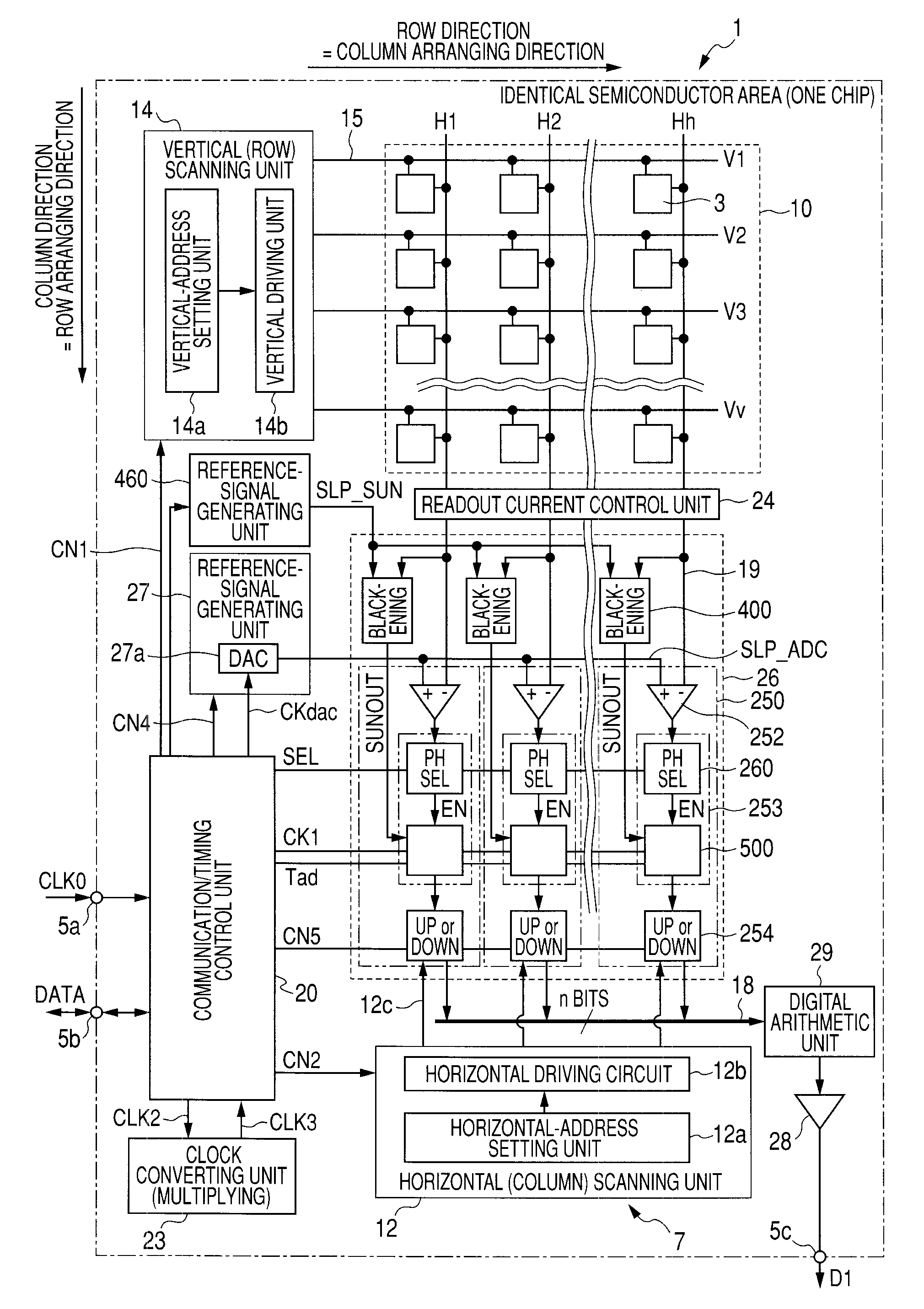
[0095]Control pulses are inputted to the counter units 254 from the horizontal scanning unit 12 through the control lines 12c. The counter units 254 have a latch function of holding a count result. The counter units 254 hold counter output values until instructions by the control pulses are received through the control lines 12c. On output sides of the respective column AD circuits 250, according to the configuration in the first embodiment, outputs of the counter units 254 are directly connected to the horizontal signal lines 18.

[0096]In such a configuration, the column AD circuits 250 perform count operations in a predetermined pixel signal readout period and output count results at predetermined timing. First, the voltage comparing units 252 compare the reference signal SLP_ADC from the reference-signal generating unit 27 and the pixel signal voltage Vx inputted through the vertical signal lines 19. When the reference signal SLP_ADC and the pixel signal voltage Vx are the same, t...

second embodiment

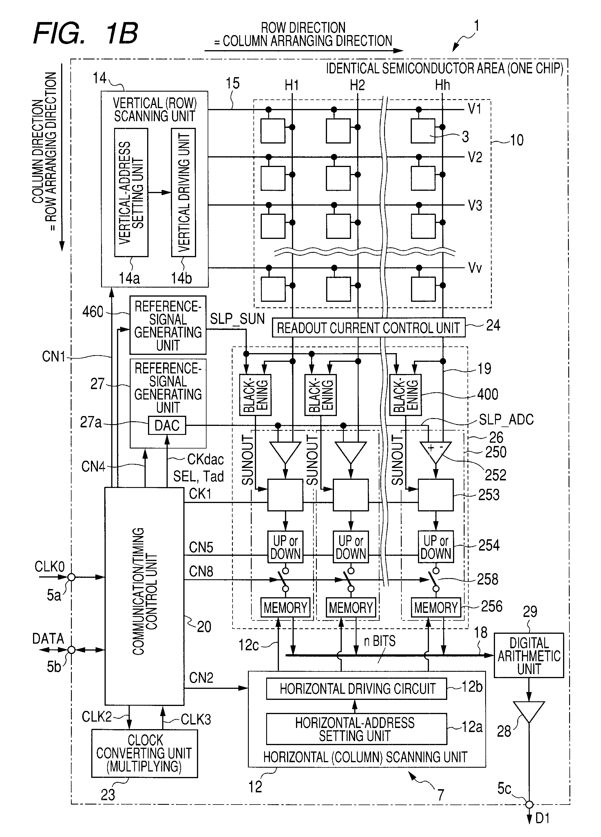
[0109]The column AD circuits 250 include, at a post-sage of the counter units 254, data storing units 256 as n-bit memory devices that store count results held by the counter units 254 and switches 258 arranged between the counter units 254 and the data storing units 256.

[0110]When the column AD circuits 250 include the data storing units 256, a memory transfer instruction pulse CN8 as a control pulse is supplied in common to the switches 258 from the communication / timing control unit 20 at predetermined timing. When the memory transfer instruction pulse CN8 is supplied, the switches 258 transfer count values of the counter units 254 corresponding thereto to the data storing units 256. The data storing units 256 hold and store the transferred count values.

[0111]A mechanism for causing the data storing units 256 to hold the count values of the counter units 254 at the predetermined timing is not limited to the configuration in which the switches 258 are arranged between both the uni...


PUM


Abstract

A solid-state imaging device includes a pixel array unit configured by arranging plural unit pixels including charge generating units and output transistors that output processing object signals corresponding to charges generated by the charge generating units, an imaging-condition determining unit that determines whether a large light-amount imaging condition, when an amount of light larger than that of light representing a saturation level is made incident on the charge generating units, is satisfied, and a control unit that performs control, on condition that the imaging-condition determining unit determines that the large light-amount imaging condition is satisfied, to correct an output signal based on processing object signals outputted from the unit pixels such that a harmful effect due to the large light-amount imaging condition is suppressed in the output signal.

Description

CROSS-REFERENCES TO RELATED APPLICATIONS[0001]The present invention contains subject matter related to Japanese Patent Application JP 2007-127099 filed in the Japanese Patent Office on May 11, 2007, the entire contents of which being incorporated herein by reference.BACKGROUND OF THE INVENTION[0002]1. Field of the Invention[0003]The present invention relates to a solid-state imaging device and an imaging apparatus, and, more particularly to a solid-state imaging device as an example of a semiconductor device for physical quantity distribution detection that is formed by arraying plural unit elements, which have sensitivity to an electromagnetic wave inputted from outside such as light and radiation, and is capable of selecting, with address control, a physical quantity distribution converted into an electric signal by the unit elements and reading out the physical quantity distribution as the electric signal and an imaging apparatus including a mechanism same as that of the solid-st...

Claims


Application Information

Patent Timeline
IPC IPC(8): H04N5/217H04N5/335H04N5/357H04N5/374H04N5/378
CPCH04N5/351H04N5/378H04N5/374H04N5/3598H04N25/50H04N25/627H04N25/76H04N25/75H04N23/70H04N23/75
Inventor MAEDA, NORIYANAKAYAMA, HIDEOOKUMURA, KENICHITAKATORI, NOZOMU
Owner SONY CORP
Why Eureka
Try Eureka