Substrate processing apparatus

a processing apparatus and substrate technology, applied in the direction of grinding machines, manufacturing tools, edge grinding machines, etc., can solve the problems of poor efficiency of operators, no attention to the accessibility of bevel polishing devices for operators, and difficulty in polishing substrates, etc., to improve the process efficiency of polishing substrates, short time period, and efficient maintenance operation

Inactive Publication Date: 2009-01-15
EBARA CORP
View PDF2 Cites 226 Cited by
  • Summary
  • Abstract
  • Description
  • Claims
  • Application Information

AI Technical Summary

Benefits of technology

[0010]The present invention has been made in view of the above drawbacks. It is, therefore, a first object of the present invention to provide a substrate processing apparatus which has an improved process efficiency of polishing a substrate, allows maintenance operation to be efficiently conducted in a short time of period, and can reduce loads of maintenance operation.
[0011]A second object of the present invention is to provide a substrate polishing method which can improve a process efficiency of polishing a substrate, allows maintenance operation to be efficiently conducted in a short time of period, and can reduce loads of maintenance operation.
[0012]A third object of the present invention is to provide a substrate processing method which can improve a process efficiency of polishing a substrate, allows maintenance operation to be efficiently conducted in a short time of period, and can reduce loads of maintenance operation.

Problems solved by technology

One of the major problems in managing particles is dust caused by surface roughness produced at a peripheral portion (a bevel portion and an edge portion) of a substrate, such as a semiconductor wafer, in a manufacturing process of semiconductor devices.
Thus, no attention is paid to the accessibility of an operator to bevel polishing devices or notch polishing devices in the polishing units when the operator replaces polishing tapes or polishing pads.
Accordingly, the operator has to work with a poor efficiency.
Further, if a polishing liquid such as slurry or abrasive particles scatter at the time of polishing by a polishing unit, the polishing liquid or the abrasive particles may contaminate respective portions in the polishing unit or a polished wafer to cause further contamination of other areas to which the polished wafer is transferred.
Thus, maintenance operation becomes a heavy load on an operator.

Method used


Image

  • Substrate processing apparatus
  • Substrate processing apparatus
  • Substrate processing apparatus

Examples


first embodiment

5. FIRST EMBODIMENT OF POLISHING UNIT

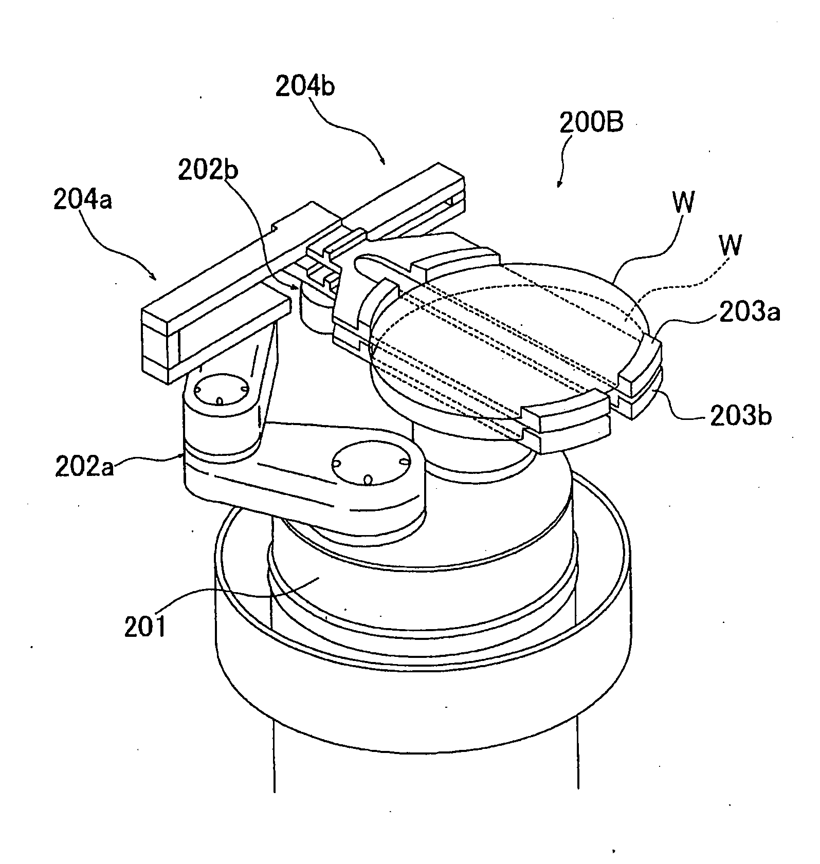
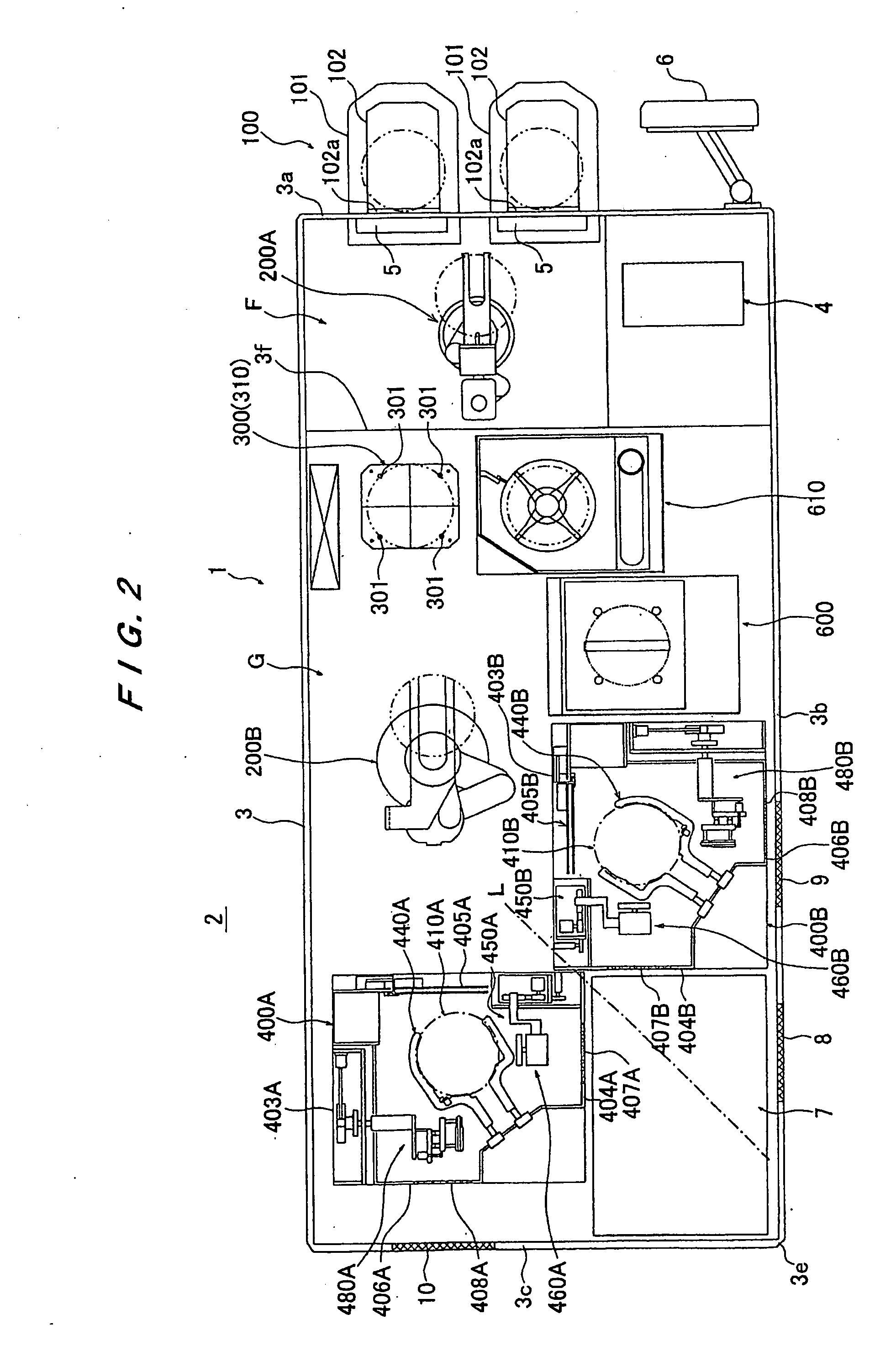
[0121]Next, structures of the first polishing unit 400A and the second polishing unit 400B will be described below. The first and second polishing units 400A and 400B have common structures. As shown in FIG. 2, respective components in casings of the first polishing unit 400A and the second polishing unit 400B are arranged symmetrically with respect to a center line L indicated by a dashed line. Specifically, the center line L is an axis of axial symmetry. The structures common to the first and second polishing units 400A and 400B will be described.

[0122]FIG. 12 is a schematic plan view showing a polishing unit 400-1 according to a first embodiment of the present invention. FIG. 13 is a cross-sectional side view of FIG. 12. FIG. 14 is a cross-sectional side view taken along a direction perpendicular to the cross-section of FIG. 13. As shown in FIGS. 12, 13, and 14, the polishing unit 400-1 has a casing 403, which defines a polishing chamber 401 a...

second embodiment

6. SECOND EMBODIMENT OF POLISHING UNIT

[0172]Another example of the polishing unit 400 will be described below. FIG. 23 is a schematic plan view of a polishing unit 400-2 according to a second embodiment of the present invention. FIG. 24 is a cross-sectional side view schematically showing a portion of the polishing unit 400-2 shown in FIG. 23. In the polishing unit 400-2, similar portions to those of the polishing unit 400-1 are denoted by the same reference numerals and will not be described repetitively. The following description relates mainly to differences between the polishing unit 400-2 and the polishing unit 400-1.

[0173]The polishing unit 400-2 has a substrate holding and rotating mechanism 550 for holding and rotating a wafer, a substrate transfer mechanism 565 for receiving, centering, and delivering the wafer, a bevel polishing device 560 for polishing a bevel portion of the wafer, a notch polishing device 580 for polishing a notch of the wafer, and a notch sensor (not sh...


PUM

PropertyMeasurementUnit
lengthaaaaaaaaaa
average particle diameteraaaaaaaaaa

Abstract

A substrate processing apparatus (1) has a first polishing unit (400A) and a second polishing unit (400B) for polishing a peripheral portion of a substrate. Each of the two polishing units (400A, 400B) includes a bevel polishing device (450A, 450B) for polishing a peripheral portion of a substrate and a notch polishing device (480A, 480B) for polishing a notch of a substrate. The substrate processing apparatus (1) has a maintenance space (7) formed between the two polishing units (400A, 400B). The bevel polishing devices (450A, 450B) in the two polishing units (400A, 400B) face the maintenance space (7) so as to be accessible from the maintenance space (7).

Description

TECHNICAL FIELD[0001]The present invention relates to a substrate processing apparatus, and more particularly to a substrate processing apparatus having a polishing unit for polishing a peripheral portion of a substrate such as a semiconductor wafer. The present invention also relates a substrate processing method, and more particularly to a substrate polishing method of polishing a peripheral portion of a substrate such as a semiconductor wafer.BACKGROUND ART[0002]In recent years, according to finer structures and higher integration of semiconductor devices, it has become more important to manage particles. One of the major problems in managing particles is dust caused by surface roughness produced at a peripheral portion (a bevel portion and an edge portion) of a substrate, such as a semiconductor wafer, in a manufacturing process of semiconductor devices.[0003]FIGS. 1A and 1B are enlarged cross-sectional views showing examples of a peripheral portion of a wafer W. FIG. 1A shows a...

Claims


Application Information

Patent Timeline
Patent Type & Authority Applications(United States)
IPC IPC(8): B24B9/00
CPCB24B9/065B24B21/16H01L21/67046H01L21/67092H01L21/67161H01L21/68792H01L21/67219H01L21/67766H01L21/68707H01L21/68728H01L21/6719H01L21/304
Inventor TAKAHASHI, TAMAMISHIRAKASHI, MITSUHIKOITO, KENYAINOUE, KAZUYUKIYAMAGUCHI, KENJISEKI, MASAYA
Owner EBARA CORP
Why Eureka
Try Eureka