Methods and devices for controlling thermal conductivity and thermoelectric power of semiconductor nanowires

a technology of thermal conductivity and thermoelectric power, applied in the direction of thermoelectric device junction materials, thermoelectric device manufacture/treatment, semiconductor devices, etc., can solve the problems of poor efficiency, limited use of thermoelectrics, and inaccessible nanometer scale using conventional lithographic patterning methods, and achieve the effect of improving thermoelectric efficiency

Active Publication Date: 2009-01-22
CALIFORNIA INST OF TECH
View PDF9 Cites 84 Cited by
  • Summary
  • Abstract
  • Description
  • Claims
  • Application Information

AI Technical Summary

Benefits of technology

[0046]Applicants have combined experiment and theory to demonstrate that semiconductor nanowires can be designed to achieve enhancements in thermoelectric efficiency, and have shown that the temperature of maximum efficiency may be tuned by changing the doping and the nanowire size. Theory indicates that similar improvements should be achievable for other semiconductor nanowire systems because of phonon effects. These nanowire thermoelectrics may find applications related to on-chip heat recovery, cooling, and power generation. Additional improvements through further optimization of nanowire size, doping, composition, etc., should be possible.

Problems solved by technology

The nanometer scale is not easily accessible using conventional lithographic patterning methods found in the microelectronic industry.
As a result, thermoelectrics find only limited use because of their poor efficiency.
Finding a material with a ZT>1, however, is challenging because optimizing one physical parameter often adversely affects another.
This behavior is due to phonon drag.
This results in an extra amount of electronic carriers diffusing down the temperature gradient and a larger voltage develops than would otherwise normally occur if phonon drag was absent.
Phonon drag, therefore, leads to a larger thermoelectric power.
Phonon drag has long been known to occur in low-doped semiconductors whose electrical conductivity is poor.
Therefore, phonon drag has not been successfully exploited in a practical thermoelectric devices since the low electrical conductivity reduces ZT.
A large doping concentration will result in a large electrical conductivity.
In contrast, a low doping concentration will result in a low electrical conductivity.
This is no easy task for commercially available thermoelectric devices, a majority of which consist of exotic materials.
Unfortunately, bulk silicon is characterized by a large thermal conductivity, and this limits the ZT of silicon to near 0.01.
The small ZT precludes the use of bulk silicon thermoelectric devices from entering the commercial market.
Silicon, for example, has a thermal conductivity ˜150 W m−1 K−1 at room temperature making it impractical for commercial use.
However, the materials used in these studies are expensive and rare, and it is not always possible to achieve high efficiencies for both p- and n-type conductors.
It is not always straightforward to even prepare both p- and n-type conductors of these systems.
It is often difficult to dope a semiconductor both p- and n-type.
It can also be difficult to precisely control the doping concentration.
In summary, the majority of bulk semiconductors are typically poor thermoelectrics either due to their large thermal conductivity and / or small electrical conductivity.
Also, current thermoelectric devices do not take advantage of phonon drag effects.

Method used


Image

  • Methods and devices for controlling thermal conductivity and thermoelectric power of semiconductor nanowires
  • Methods and devices for controlling thermal conductivity and thermoelectric power of semiconductor nanowires
  • Methods and devices for controlling thermal conductivity and thermoelectric power of semiconductor nanowires

Examples


Embodiment Construction

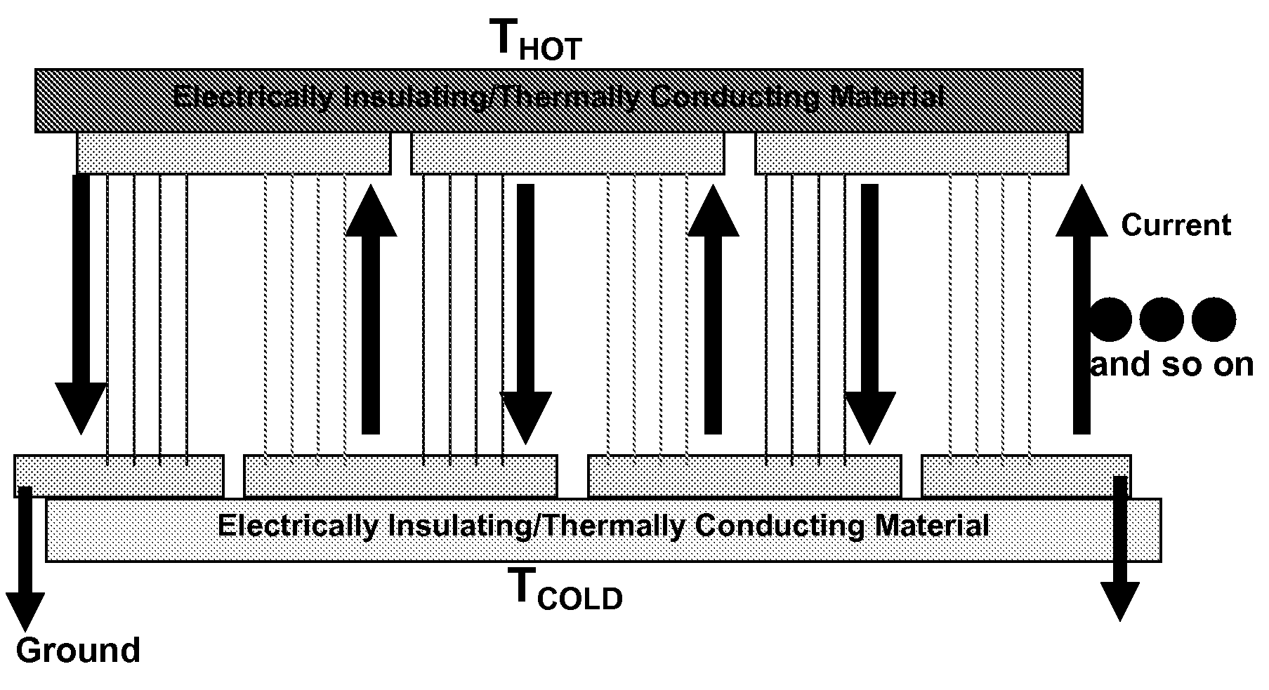
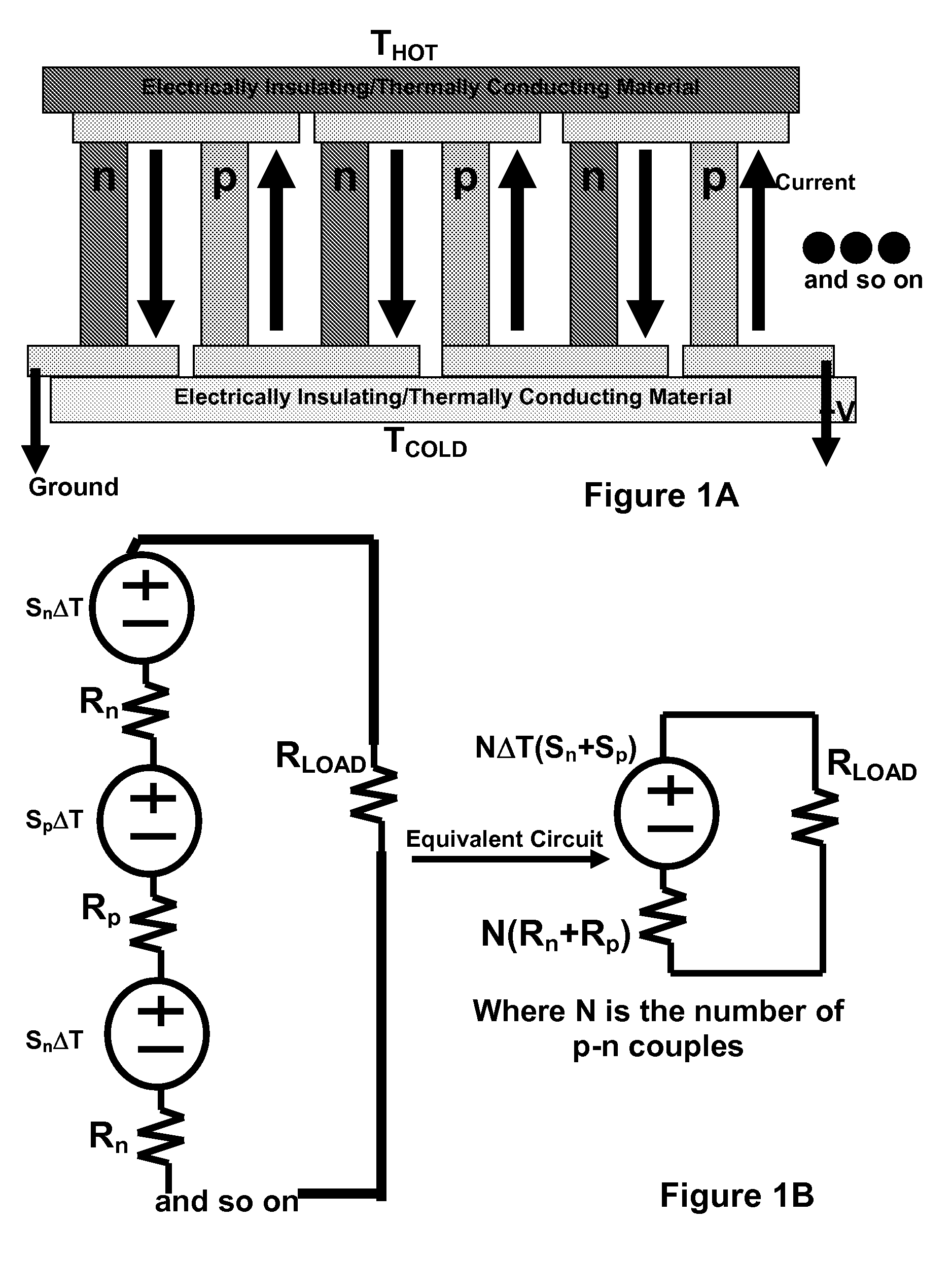
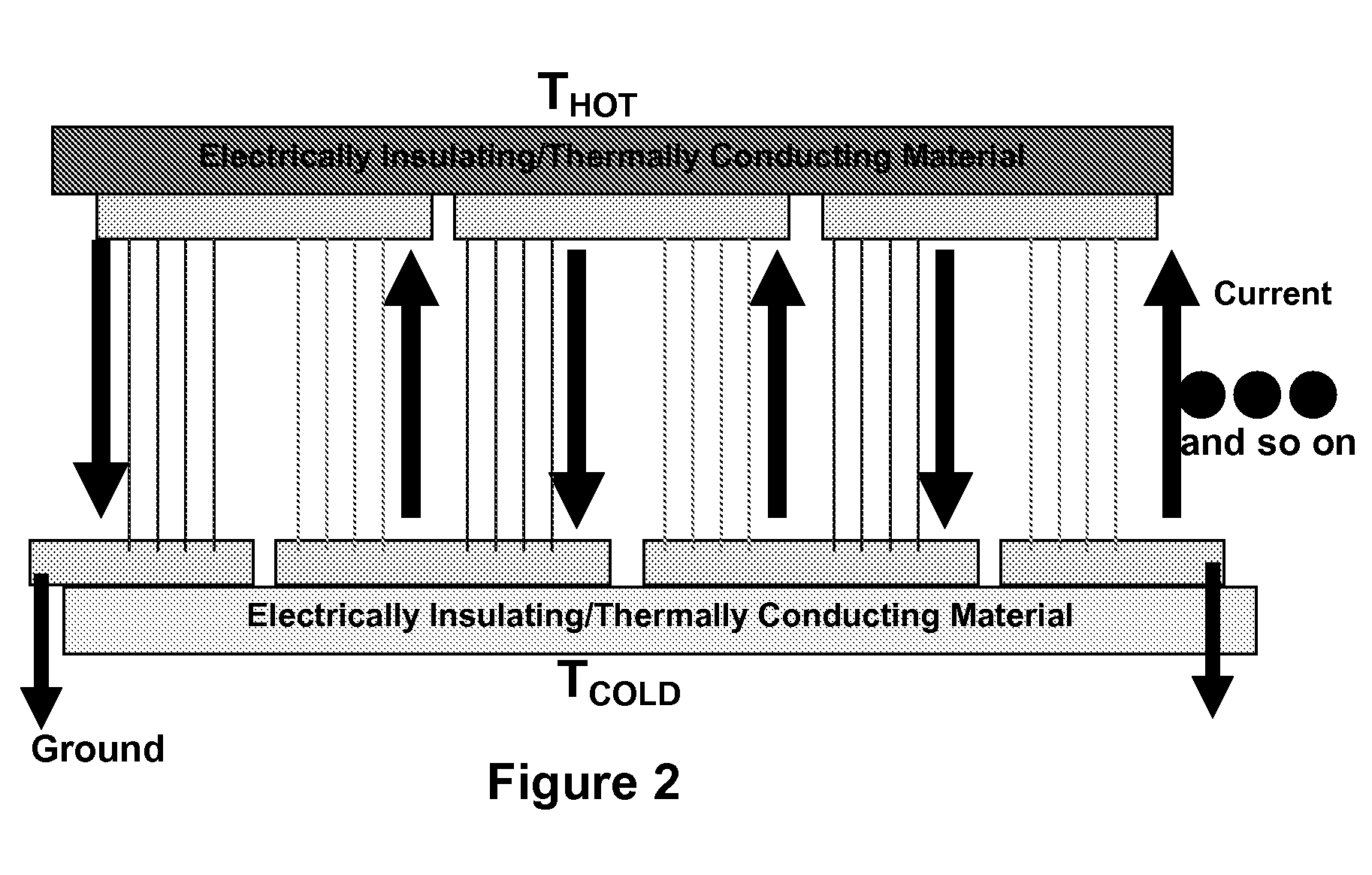
[0056]For the very simple system of silicon nanowires, Applicants found that by tuning the nanowires' dimensions, the thermal conductivity is dramatically reduced, while maintaining a high electrical conductivity. Furthermore, Applicants have also found that the thermopower in highly doped (good electrically conducting) nanowires can be increased further by phonon drag. The thermopower depends upon nanowire diameter, nanowire length, and impurity doping. The thermal conductivity depends upon just nanowire diameter. Thus, the present application provides a thermoelectric device that removes the interdependency of the three thermoelectric material parameters that govern ZT. Applicants used silicon nanowires as an example to engineer an excellent thermoelectric material. Silicon is just one example of of a semiconducting nanowire material that can be used to fabricate a high efficiency thermoelectric device. Other semiconductor materials such as germanium and alloys of silicon and germ...


PUM

PropertyMeasurementUnit
thermal conductivityaaaaaaaaaa

Abstract

Methods and devices for controlling thermal conductivity and thermoelectric power of semiconductor nanowires are described. The thermal conductivity and the thermoelectric power are controlled substantially independently of the electrical conductivity of the nanowires by controlling dimensions and doping, respectively, of the nanowires. A thermoelectric device comprising p-doped and n-doped semiconductor nanowire thermocouples is also shown, together with a method to fabricate alternately p-doped and n-doped arrays of silicon nanowires.

Description

CROSS REFERENCE TO RELATED APPLICATIONS[0001]The present application claims the priority benefit of U.S. Provisional Application No. 60 / 961,395 filed on Jul. 20, 2007 for “High Performance Semiconductor Nanowire Thermoelectrics” by James R Heath, Akram Boukai, Yuri Bunimovich, William A Goddard, and Jamil Tahir-Kheli, the contents of which are herein incorporated by reference in their entirety.STATEMENT OF GOVERNMENT GRANT[0002]The U.S. Government has certain rights in this invention pursuant to Grant No. DE-FG02-04ER46175 awarded by DOE, Grant No. CCF0524490 awarded by National Science Foundation and Grant No. N00014-07-1-0360 & N00014-06-1-0938 awarded by the Office of Naval Research.BACKGROUND[0003]1. Field[0004]The present disclosure relates to thermoelectric devices and related fabrication methods. More in particular, it relates to methods and devices for controlling thermal conductivity and thermoelectric power of semiconductor nanowires. It also relates to electric power gene...

Claims


Application Information

Patent Timeline
Patent Type & Authority Applications(United States)
IPC IPC(8): H01L35/34H01L35/00
CPCH01L35/26H01L35/32H01L35/34H01L2924/0002H01L2924/00H10N10/857H10N10/17H10N10/01
Inventor BOUKAI, AKRAMBUNIMOVICH, YURIGODDARD, WILLIAM A.HEATH, JAMES R.TAHIR-KHELI, JAMIL
Owner CALIFORNIA INST OF TECH
Why Eureka
Try Eureka