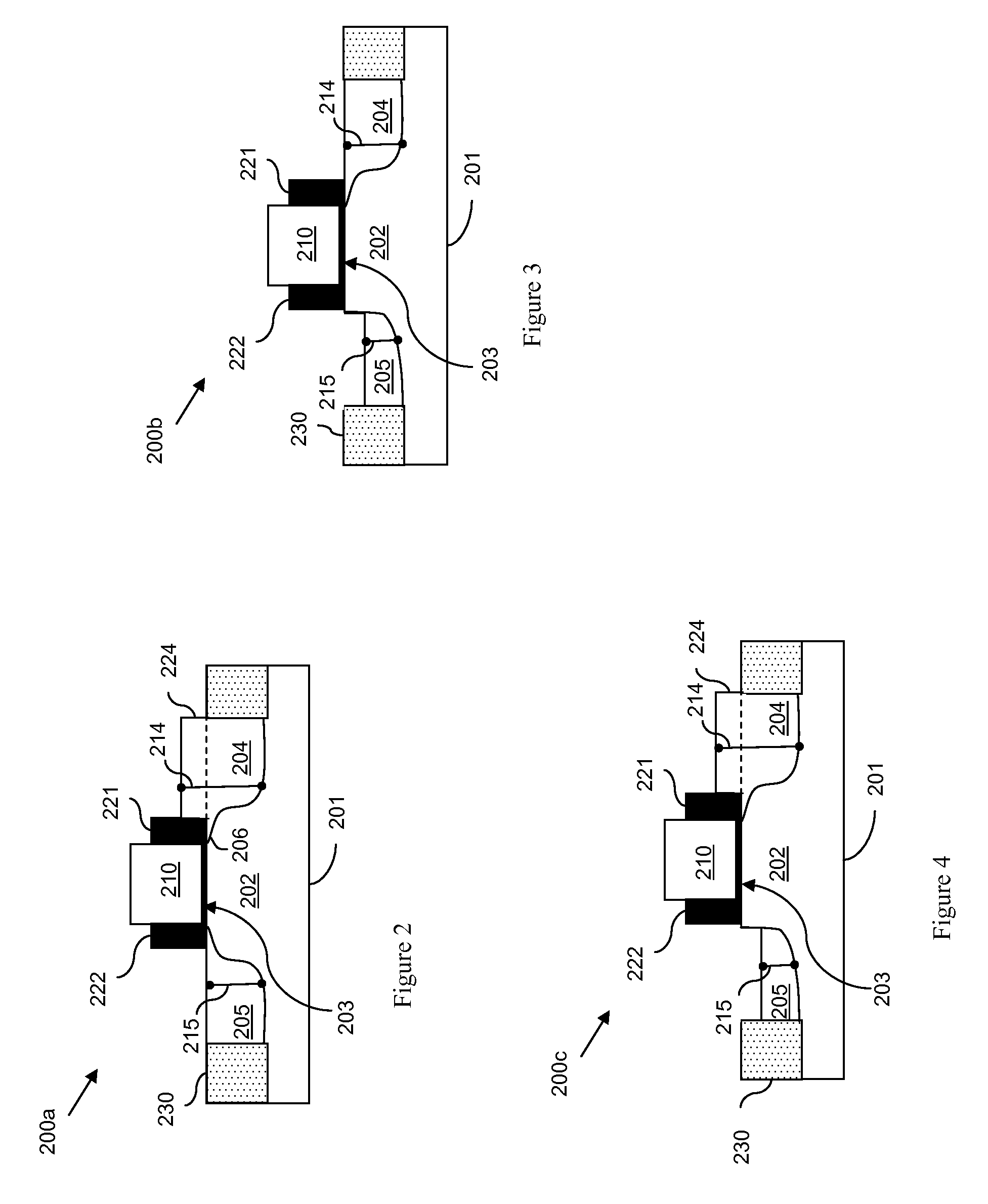
[0010]In this embodiment, in addition to having different heights, the source and drain regions of the
transistor structure can further be separated from the gate
electrode by different distances in order to further minimize series resistance in the source region as well as to further minimize gate to drain capacitance. Specifically, the source region can have one height relative to the top surface of the channel region and the drain region can have a different lesser height relative to the top surface of the channel region. Additionally, the source region can be separated from the gate
electrode by one distance and the drain region can be separated from the gate
electrode by a different greater distance. This asymmetric configuration allows for additional tailoring of the series resistance
and gate to drain capacitance (i.e., allows for even greater simultaneous minimization of series resistance in the source region and gate to drain capacitance) over asymmetric source and drain heights alone. More specifically, the values of the height of the source region, the height of the drain region, the distance between the source and gate and the distance between the drain and gate can be tailored to ensure that series resistance in the source region is less than a predetermined resistance value and to simultaneously ensure that gate to drain capacitance is less than a predetermined capacitance value.
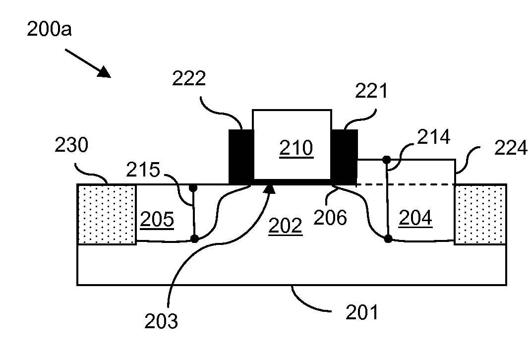
[0012]Separation of the source and drain regions from the gate electrode by different predetermined distances can, for example, be accomplished by means of gate sidewall spacers having different predetermined widths. That is, the
transistor structure can further comprise a sidewall spacer adjacent to the source-side of the gate electrode. This source-side sidewall spacer can comprise a
nitride sidewall spacer having a predetermined width that is approximately equal to the desired distance between the source region and the source-side of the gate electrode. The transistor structure can also further comprise another sidewall spacer adjacent to the drain-side of the gate electrode. This drain-side sidewall spacer can similarly comprise a
nitride sidewall spacer. However, the predetermined width of the drain-side sidewall spacer can be greater than that of the source-side sidewall spacer. That is, the drain-side sidewall spacer can be approximately equal to the desired distance between the drain region and the drain-side of the gate electrode. Then, during formation, the gate sidewall spacer widths can be used to effectively control positioning of the source and drain dopants during implantation. Thus, the values of the different heights of the source and drain regions and the different sidewall spacer widths (representing the different distances between the source and drain regions and the gate) can be tailored to ensure that series resistance in the source region is less than a predetermined resistance value and to simultaneously ensure that gate to drain capacitance is less than a predetermined capacitance value.
[0014]This method embodiment can further comprise predetermining the height of the source region and the height of the drain region relative to the top surface of the channel region. Specifically, this predetermining process can comprise tailoring the height of the source region and the height of the drain region so that the height of the drain region is less than the height of the source region. This asymmetric configuration allows series resistance in the source region and gate to drain capacitance to be simultaneously minimized. More specifically, the different heights of the source and drain regions can be tailored so that series resistance in the source region is less than a predetermined resistance value and so that gate to drain capacitance is less than a predetermined capacitance value.
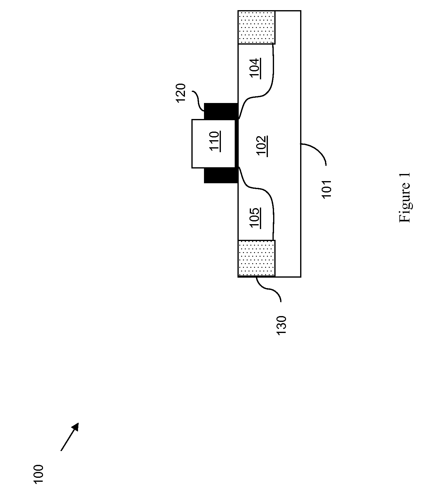
[0018]It should be noted that, during the deep source and drain
implant processes, the widths of the gate sidewall spacers control the positioning of the deep source region and deep drain region, relative to the gate electrode. In this embodiment, the gate sidewall spacers are formed symmetrically. Thus, the source and drain regions will be separated from the gate electrode by the same distance (i.e., by a distance that is approximately equal to the sidewall spacer width).
[0020]This method embodiment further comprises predetermining not only different heights for the source and drain regions relative to the top surface of the channel region, but also predetermining different distances between the source and drain regions and the gate electrode in order to simultaneously minimize series resistance in the source region and gate to drain capacitance. That is, this method embodiment comprises predetermining each of the following: the height of the source region, the height of the drain region, the distance between the source region and one side of the gate electrode, and the distance between the drain region and the opposite side of the gate electrode. The heights of the source and drain regions are predetermined relative to the top surface of the channel region. Specifically, this predetermining process can comprise tailoring the different heights of the source and drain regions and the different distances between the source and drain regions and the gate so that the height of the drain region is less than the height of the source region and also so that the distance between the drain region and the gate is greater than the distance between the source region and the gate. This asymmetric configuration allows for additional tailoring of the series resistance and gate to drain capacitance (i.e., allows for even greater simultaneous minimization of series resistance in the source region and gate to drain capacitance) over the transistor configurations with asymmetric source and drain heights alone. More specifically, the different predetermined heights and different predetermined distances can be tailored so that series resistance in the source region is less than a predetermined resistance value and so that gate to drain capacitance is less than a predetermined capacitance value.

