Multi-doped slab silicon optical modulator

a silicon optical modulator and slab technology, applied in non-linear optics, instruments, optics, etc., can solve the problems of large bandwidth demand, limited popular applications, and small amount of data transferred, and achieve the effect of reducing series resistan

Pending Publication Date: 2022-06-09
MARVELL ASIA PTE LTD
View PDF0 Cites 1 Cited by
  • Summary
  • Abstract
  • Description
  • Claims
  • Application Information

AI Technical Summary

Benefits of technology

[0015]Optionally, the multiple P-type doped sections and the multiple N-type doped sections are configured to optimize respective lengths and doping levels for corresponding sections with respective distances from the rib structure to minimize series resistances through respective total lengths of the first slab region and the second slab region.
[0023]P-type doping level away from the P-type part of rib structure towards the P++ region and forming multiple sections in the second slab region with increasing N-type doping level away from the N-type part of rib structure towards the N++ region includes optimizing different lengths and doping levels for different sections with corresponding distances away from the rib structure to minimize series resistances in the first slab region and the second slab region while without causing extra optical loss.

Problems solved by technology

In the early days Internet, popular applications were limited to emails, bulletin board, and mostly informational and text-based web page surfing, and the amount of data transferred was usually relatively small.
Today, Internet, social network, mobile applications, and cloud computing demand a huge amount of bandwidth for transferring large amount of data such as photo, video, music, and other multimedia files.

Method used


Image

  • Multi-doped slab silicon optical modulator
  • Multi-doped slab silicon optical modulator
  • Multi-doped slab silicon optical modulator

Examples


Embodiment Construction

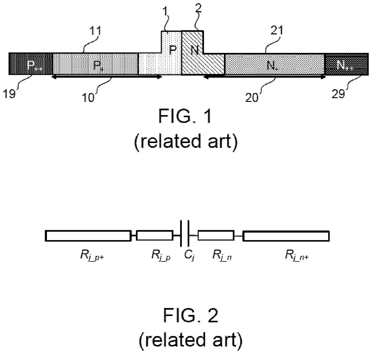
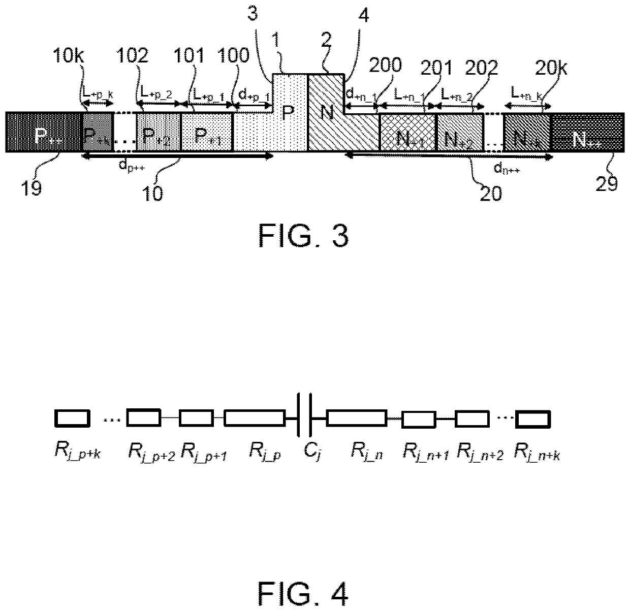
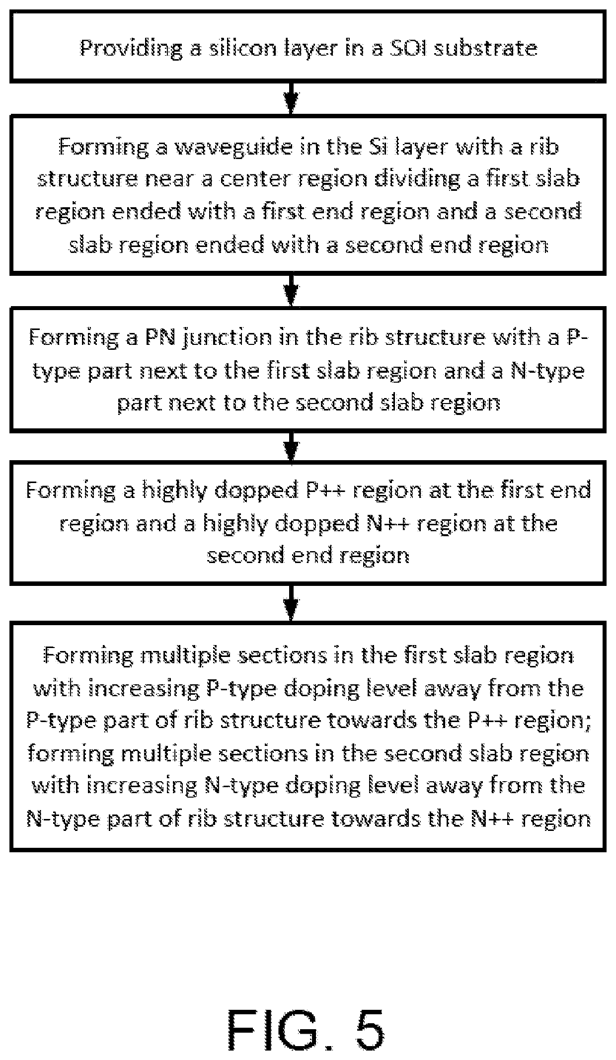
[0031]The present invention relates to optical telecommunication techniques. More particularly, the present invention provides an improved silicon optical modulator based multi-doped slab region to decrease the series resistance and enhance modulation bandwidth without sacrificing modulation efficiency or adding extra loss, applicable in various electro-optical modulator configurations in photonics system, though other applications are possible.

[0032]The following description is presented to enable one of ordinary skill in the art to make and use the invention and to incorporate it in the context of particular applications. Various modifications, as well as a variety of uses in different applications will be readily apparent to those skilled in the art, and the general principles defined herein may be applied to a wide range of embodiments. Thus, the present invention is not intended to be limited to the embodiments presented, but is to be accorded the widest scope consistent with t...


PUM

PropertyMeasurementUnit
total lengthaaaaaaaaaa
electrical resistancesaaaaaaaaaa
cross-sectional dimensionaaaaaaaaaa

Abstract

A silicon optical modulator with improved bandwidth includes a silicon waveguide with a rib structure in cross section connected to a first slab region and a second slab region respectively on two opposite sides of the rib structure. The silicon optical modulator further includes a PN junction formed in the rib structure with a P-type part joined with the first slab region and a N-type part joined with the second slab region. Additionally, the silicon optical modulator includes multiple P-type doped sections formed one next to another in the first slab region ended with a first end region and multiple N-type doped sections one next to another formed in the second slab region ended with a second end region. The multiple P-type or N-type doped sections are configured with increasing doping levels for sections further away from the rib structure.

Description

CROSS-REFERENCE TO RELATED APPLICATIONS[0001]N / ABACKGROUND OF THE INVENTION[0002]The present invention relates to optical communication techniques. More particularly, the present invention provides a silicon optical modulator, a method for forming the silicon optical modulator with improved modulator bandwidth.[0003]Over the last few decades, the use of communication networks exploded. In the early days Internet, popular applications were limited to emails, bulletin board, and mostly informational and text-based web page surfing, and the amount of data transferred was usually relatively small. Today, Internet, social network, mobile applications, and cloud computing demand a huge amount of bandwidth for transferring large amount of data such as photo, video, music, and other multimedia files. Most of traffic is coming from the consumer usage. For example, a social network like Facebook processes more than 500 TB of data daily. With such high demands on data and data transfer with hi...

Claims


Application Information

Patent Timeline
Patent Type & Authority Applications(United States)
IPC IPC(8): G02F1/025G02F1/015
CPCG02F1/025G02F2201/063G02F2202/06G02F1/0152
Inventor KARIMELAHI, SAMIRAKATO, MASAKI
Owner MARVELL ASIA PTE LTD
Why Eureka
Try Eureka