Interdigitated multi-pixel arrays for the fabrication of light-emitting devices with very low series-resistances and improved heat-sinking

a light-emitting device and multi-pixel array technology, which is applied in the manufacture of electric discharge tubes/lamps, lighting and heating apparatuses, and discharge tubes luminescnet screens. it can solve the problems of limited light-emitting wavelength (i.e., its color), high current operation, and high output power of high-brightness light-emitting devices. achieve the effect of minimizing series resistance, improving heat-sinking, and minimizing series resistan

Active Publication Date: 2009-04-14
RGT UNIV OF CALIFORNIA
View PDF33 Cites 0 Cited by
  • Summary
  • Abstract
  • Description
  • Claims
  • Application Information

AI Technical Summary

Benefits of technology

[0016]The present invention discloses a plurality of interdigitated pixels arranged in an array, with very low series-resistances, improved current spreading and heat-sinking, and high brightness output.
[0018]Each pixel is a square with sides of dimension l. The series resistance is minimized by increasing the perimeter of an active region for the pixels. The series resistance is also minimized by shrinking the space between a mesa and n-contact for each pixel.
[0019]Heat-sinking is improved by separating the pixels by a distance.
[0020]Current spreading is improved by shrinking the pixels' size. In addition, current spreading is improved by the interdigitated pixels' geometry.
[0021]The present invention also discloses a method of fabricating a light-emitting device, comprising fabricating a plurality of interdigitated pixels arranged in an array, with very low series-resistances, improved current spreading and heat-sinking, and high brightness output. In addition, the present invention discloses a device fabricated according to this method.

Problems solved by technology

The wavelength of light (i.e., its color) that can be emitted by a given material of the light-emitting device is limited by the physical characteristics of that material, specifically its bandgap energy.
However, large series-resistance, because of the contacts and the bulk p-regions and n-regions of the devices, results in heating.
Moreover, high brightness light-emitting devices generally require very high output power.
This prevents high current operation because the device generates huge amount of heat with high input electrical power.
In addition, the heat generated at higher drive currents leads to the roll-off of the output power.

Method used


Image

  • Interdigitated multi-pixel arrays for the fabrication of light-emitting devices with very low series-resistances and improved heat-sinking
  • Interdigitated multi-pixel arrays for the fabrication of light-emitting devices with very low series-resistances and improved heat-sinking
  • Interdigitated multi-pixel arrays for the fabrication of light-emitting devices with very low series-resistances and improved heat-sinking

Examples


Embodiment Construction

[0037]In the following description of the preferred embodiment, reference is made to the accompanying drawings which form a part hereof, and in which is shown by way of illustration a specific embodiment in which the invention may be practiced. It is to be understood that other embodiments may be utilized and structural changes may be made without departing from the scope of the present invention.

(I) Analysis for Series Resistance

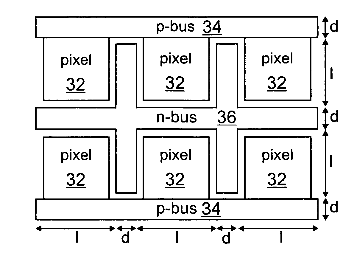
[0038]FIG. 1 illustrates a light-emitting device 10 that comprises a diode structure (i.e., a p-n junction) fabricated on a substrate or template 12 with active layers or region (such as quantum wells (QWs)) 14 embedded between p-layers or regions 16 and n-layers or regions 18. The p-layers 16 include both a p− layer 20 and p+ layer 22. The device 10 also includes a semi-transparent p-current-spreading layer (i.e., p-contact) 24, thick p-contact 26 and n-contact 28.

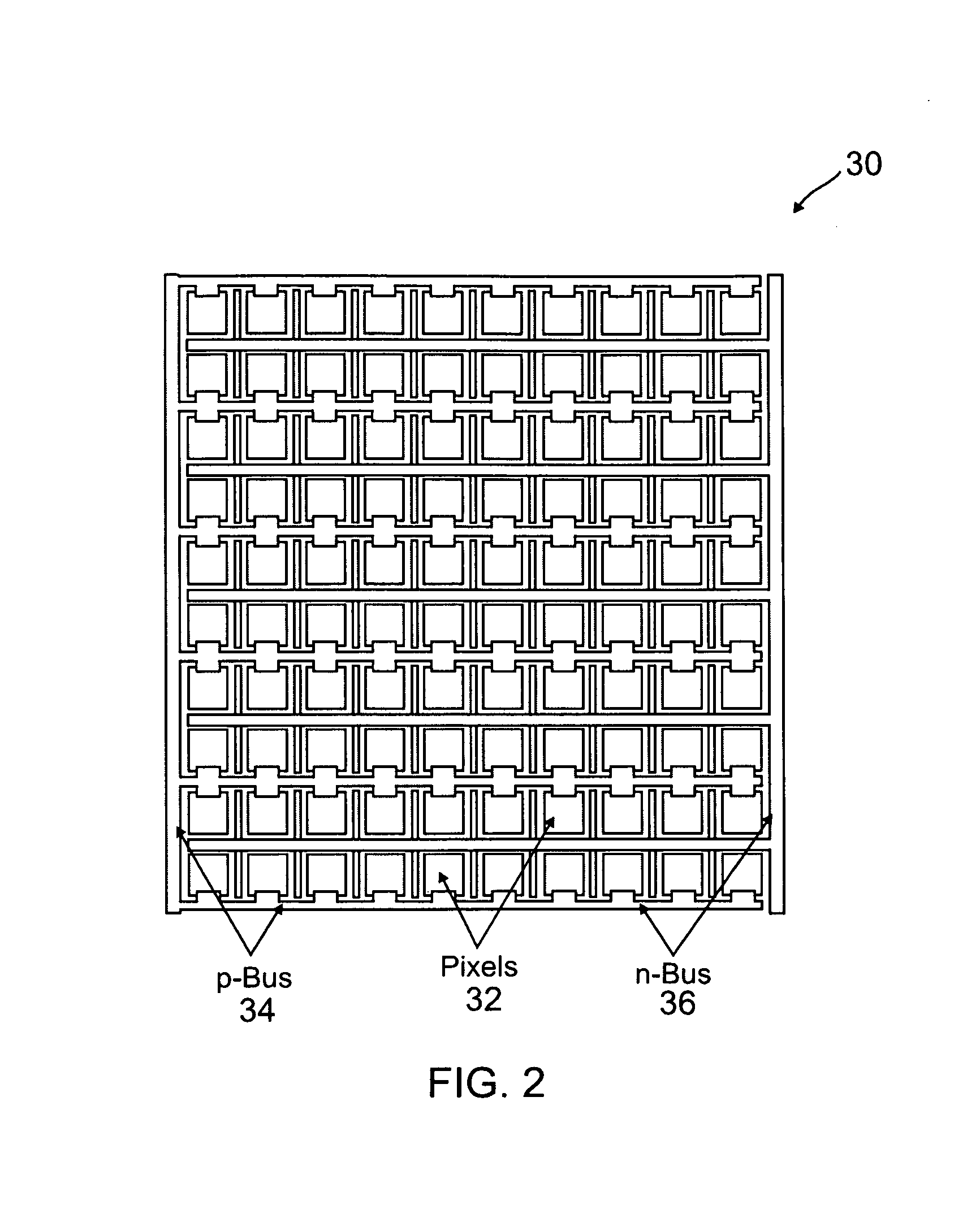
[0039]For a square-shaped light-emitting device grown on an insulating substrate, such as sho...


PUM


Abstract

The present invention discloses a plurality of interdigitated pixels arranged in an array, having a very low series-resistances with improved current spreading and improved heat-sinking. Each pixel is a square with sides of dimension l. The series resistance is minimized by increasing the perimeter of an active region for the pixels. The series resistance is also minimized by shrinking the space between a mesa and n-contact for each pixel.

Description

CROSS-REFERENCE TO RELATED APPLICATION[0001]This application claims the benefit under 35 U.S.C. § 119(e) of the following and commonly-assigned application:[0002]U.S. Provisional Application Ser. No. 60 / 624,026, filed on Nov. 1, 2004, by Arpan Chakraborty, Likun Shen and Umesh K. Mishra, entitled “INTERDIGITATED MULTI-PIXEL ARRAYS FOR THE FABRICATION OF LIGHT-EMITTING DEVICES WITH VERY LOW SERIES-RESISTANCES,”;[0003]which application is incorporated by reference herein.STATEMENT REGARDING SPONSORED RESEARCH AND DEVELOPMENT[0004]The present invention was made under support from the University of California, Santa Barbara, Solid State Lighting and Display Center member companies, including Stanley Electric Co., Ltd., Mitsubishi Chemical Corp., Rohm Co., Ltd., Cree, Inc., Matsushita Electric Works, Matsushita Electric Industrial Co., and Seoul Semiconductor Co., Ltd.BACKGROUND OF THE INVENTION[0005]1. Field of the Invention[0006]The present invention relates to high-power light-emittin...

Claims


Application Information

Patent Timeline
Patent Type & Authority Patents(United States)
IPC IPC(8): H01J1/62F21K99/00
CPCF21K9/00H01L33/62H01L33/08H01L33/14H01L27/156H01L25/0753H01L33/38H01L2924/0002H01L2924/00H01L33/48H01L33/64H01L33/20H01L33/385H01L33/42H01L33/486H01L2933/0033H01L2933/0066
Inventor CHAKRABORTY, ARPANSHEN, LIKUNMISHRA, UMESH K.
Owner RGT UNIV OF CALIFORNIA
Why Eureka
Try Eureka