

A/d converter
- Summary
- Abstract
- Description
- Claims
- Application Information
AI Technical Summary
Benefits of technology
Problems solved by technology
Method used
Image

Examples
first embodiment
[0071]A first embodiment of an A / D converter according to the present invention and a sensor system comprising the A / D converter will be described with reference to FIGS. 8 and 9.
[0072]First, a sensor system according to this embodiment will be described with reference to FIG. 8.
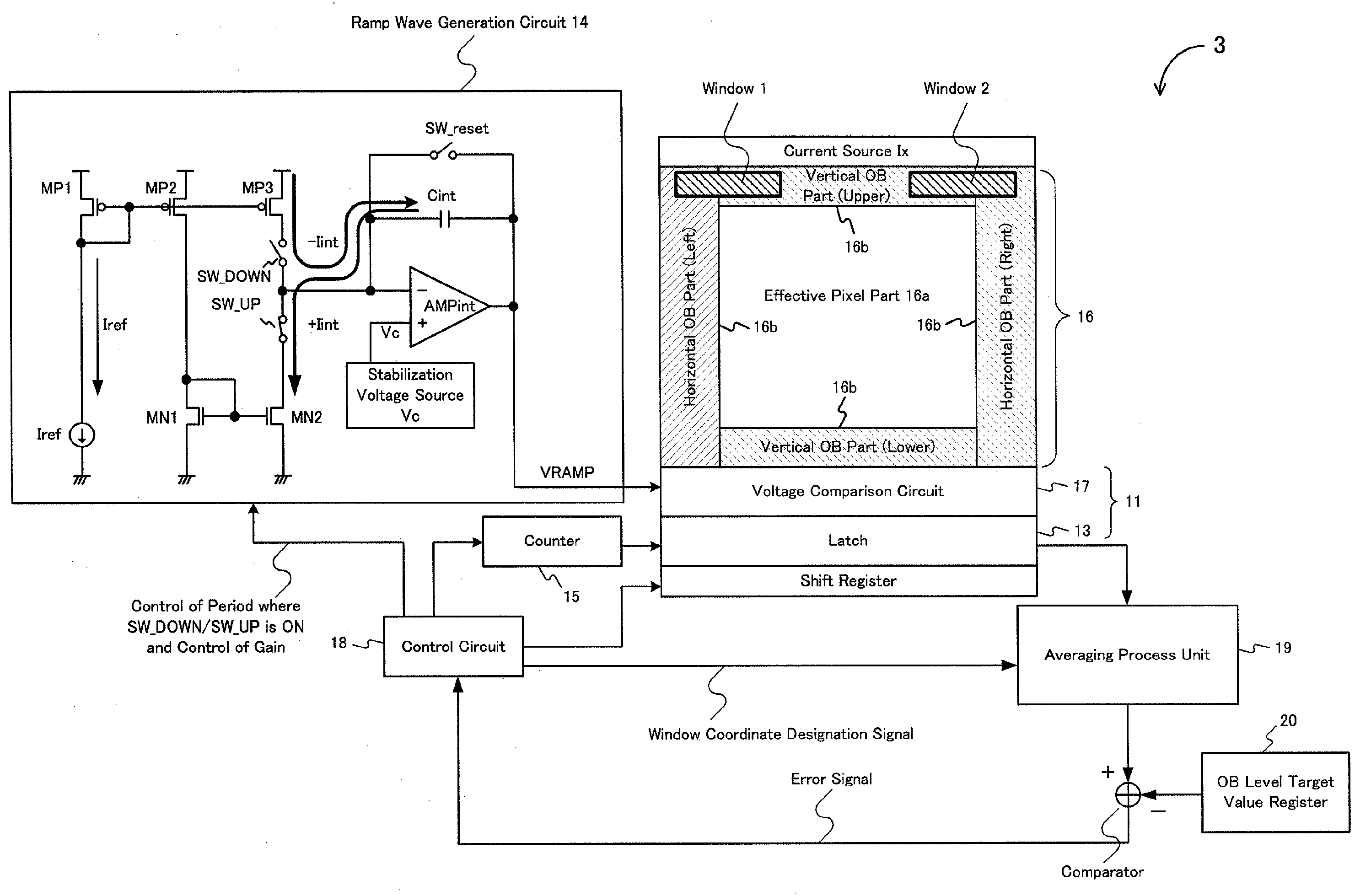
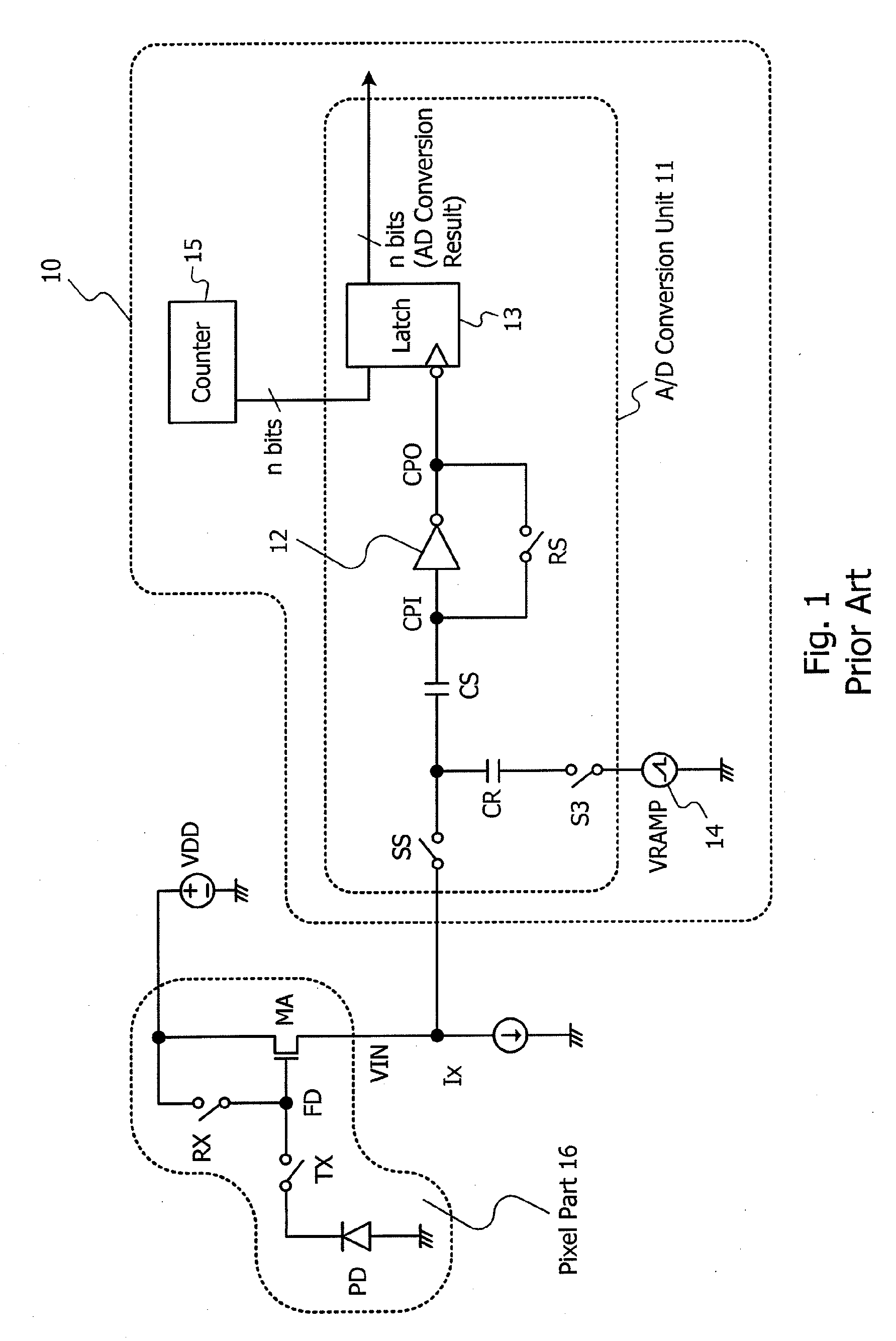
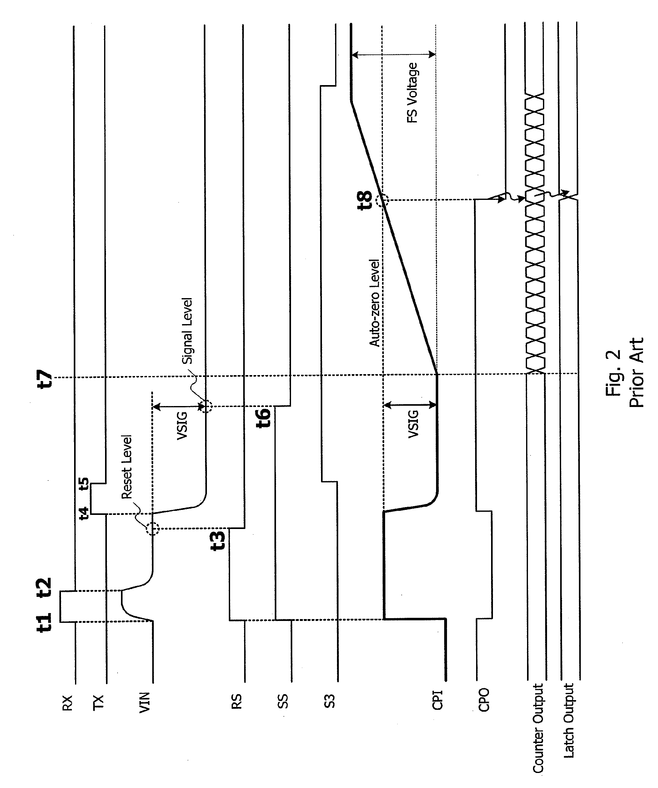
[0073]As shown in FIG. 8, a sensor system 1 comprises a pixel part (sensor unit) 16 in which a plurality of photoelectric conversion elements are arranged in the shape of a matrix, and components of the A / D converter according to the present invention. The pixel part 16 comprises an effective pixel part 16a, and an optical black pixel part (OB part) 16b provided at a part of the marginal portions of the pixel part 16. The OB part 16b is shielded from light and outputs only an analog voltage provided by a dark current, to be converted, that is, an analog voltage to be converted containing a noise component.
[0074]The A / D converter comprises, as its basic constitution, a ramp wave generation circuit (ramp volta...
second embodiment
[0088]A second embodiment of an A / D converter according to the present invention and a sensor system comprising the A / D converter will be described with reference to FIGS. 10 to 15. According to this embodiment, a description will be made of a case where control differs between cases where the OB levels (average noise voltage) are above and below the target noise voltage.
[0089]First, constitutions of an AID converter and a sensor system according to this embodiment will be described. FIG. 14 shows a schematic constitution of the sensor system 2 according to this embodiment. In addition, the basic constitutions of the A / D converter and the sensor system 2 in this embodiment are the same as those in the A / D converter and the sensor system in the first embodiment.
[0090]A control circuit 18 according to this embodiment calculates an index value showing a difference between an OB level (average noise voltage) and a target noise voltage, and calculates a counter standby time to adjust a c...
third embodiment
[0107]A third embodiment of an A / D converter according to the present invention and a sensor system comprising the A / D converter will be described with reference to FIGS. 16 and 18. Although the description has been made of the case where the counting start timing of the counter is adjusted with respect to the control reference timing in the above first and second embodiments, a description will be made of a case where the criterion level of the reference voltage at the counting start timing is adjusted in this embodiment.
[0108]First, constitutions of the A / D converter and sensor system of this embodiment will be described with reference to FIG. 18. The constitutions of the A / D converter and the sensor system in this embodiment are basically the same as those of the A / D converter and the sensor system in the first and second embodiments.
[0109]A control circuit 18 in this embodiment calculates an index value showing a difference between an OB level (average noise voltage) and a targe...
PUM
 Abstract
Description
Claims
Application Information