Semiconductor device
a technology of semiconductor chips and semiconductor chips, applied in semiconductor devices, semiconductor/solid-state device details, instruments, etc., can solve the problems of inability to supply electrical power to semiconductor chips, inability to develop and manufacture multiple types of chips to match the stacked positions, etc., and achieve the effect of reducing the cost required
- Summary
- Abstract
- Description
- Claims
- Application Information
AI Technical Summary
Benefits of technology
Problems solved by technology
Method used
Image
Examples
first embodiment
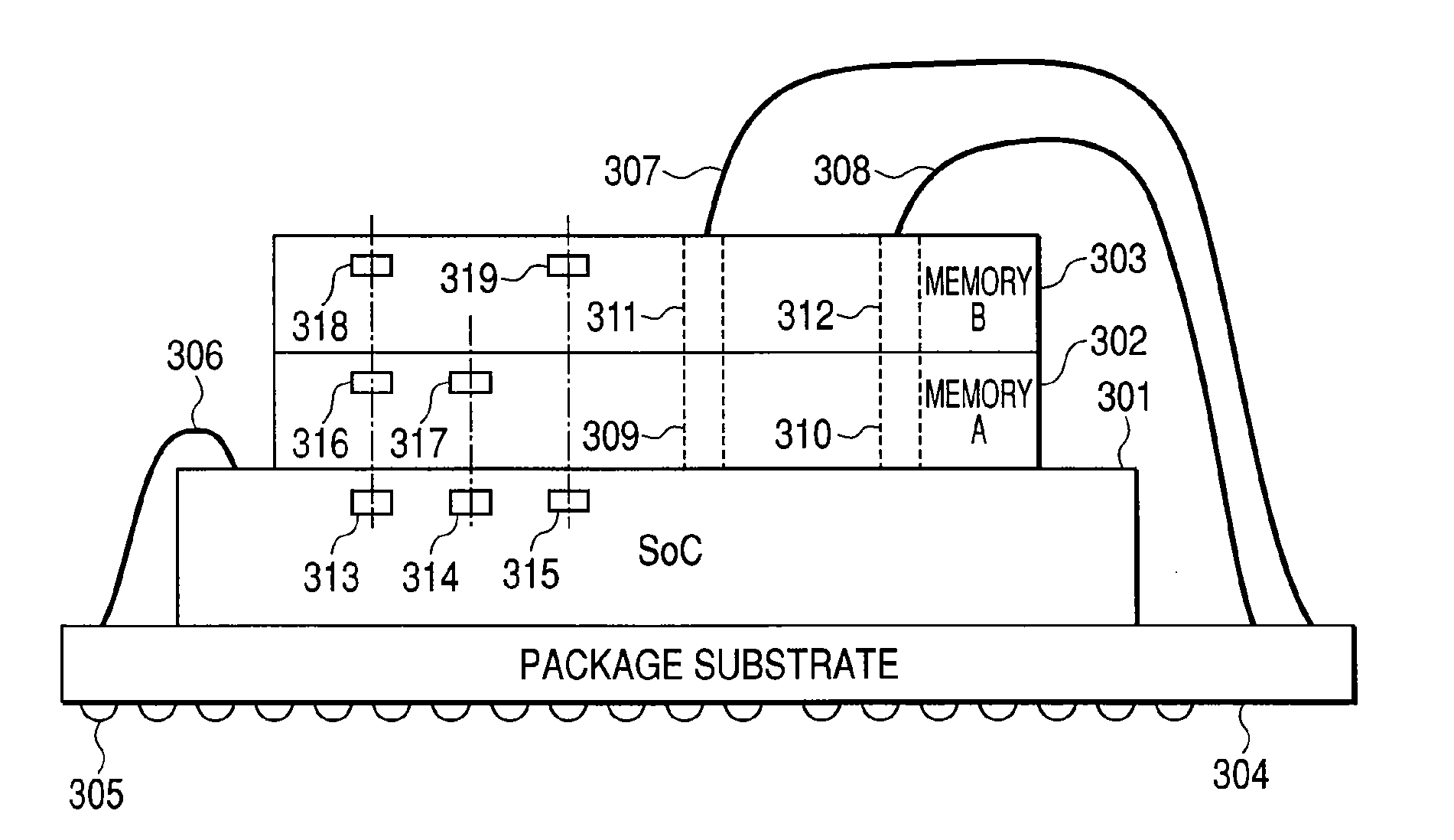
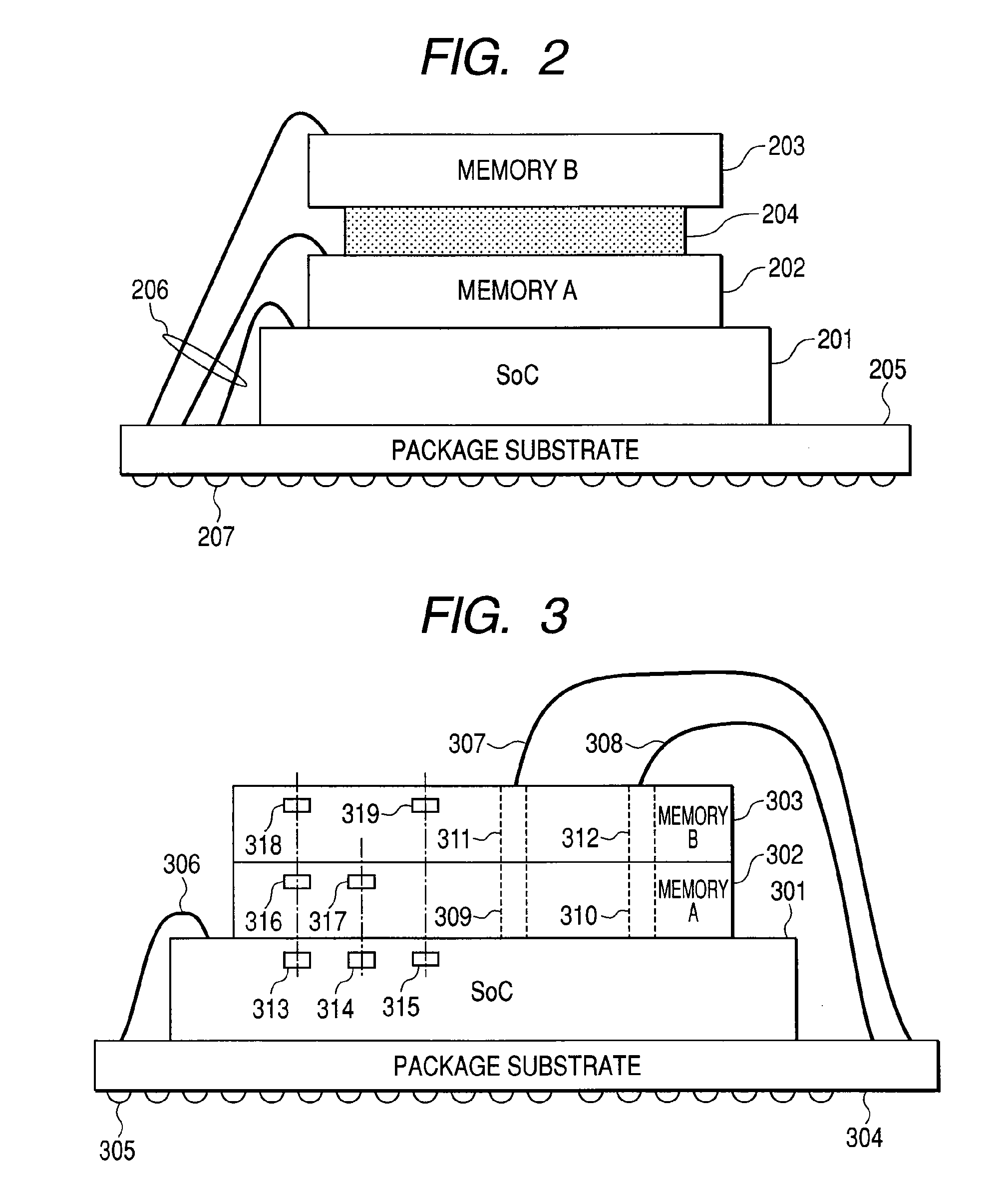
[0062]The first embodiment of this invention is stacked semiconductor integrated circuits contained in the SiP with the terminals set upwards and connected by bonding wire.
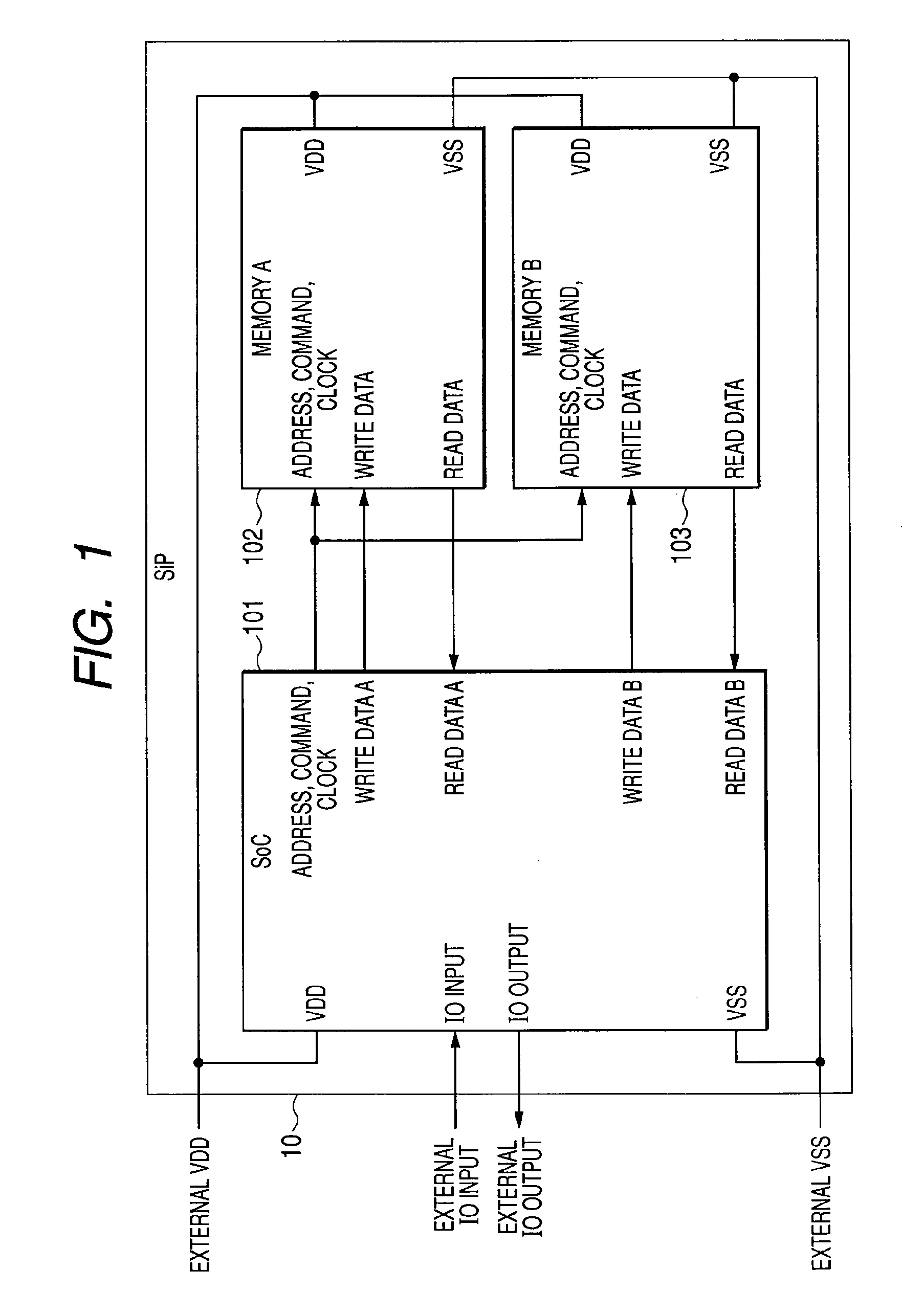
[0063]FIG. 1 is a block diagram showing the structure of the semiconductor device of the first embodiment of this invention. FIG. 1 is a logical block diagram showing the related functional connections for the System In Package (Hereafter, called SIP.) of the first embodiment of this invention.
[0064]The SiP 10 contains a SoC101, a memory A102, and a memory B103 as well as a function for communicating outside the SiP10. The SoC101 implements the applicable communication function by loading the program stored in the memory A102 and memory B103. The SoC101 also contains a function for writing on the memory A102 and the memory B103.
[0065]The SoC101 as well as memory A102 and memory B103 are semiconductor integrated circuits made for example from single crystal silicon and including CMOS (complementary MOS transistors)...
second embodiment
[0124]The second embodiment of this invention stacks the semiconductor integrated circuit face-down in the SiP. The physical structure of the SiP of the second embodiment is described next. The logical structure of the SiP of the second embodiment is identical to the logical structure of the SiP of the first embodiment.
[0125]FIG. 11 is a drawing of the semiconductor integrated circuit mounted in the SiP of the second embodiment of this invention as seen from a horizontal view.
[0126]The SoC1101, the memory A1102 and the memory B1103 are all mounted face-down in the SiP20.
[0127]The structure of the SiP20 is described first.
[0128]The SiP20 contains an SoC1101, the memory A1102 and the memory B1103, the package substrate 1104, the external terminal 1105, and the micro-bumps 1106-1108.
[0129]The SoC1101, the memory A1102, and the memory B1103 correspond to the respective SoC1101, memory A102, and memory B103 in FIG. 1.
[0130]The memory A1102 of the second embodiment is identical to the mem...
third embodiment
[0147]In the first and second embodiments, three-dimensional communication was directly performed between the SoC and memory A, and also between the SoC and memory B. However the inductive coupling coefficient is inversely proportional to the square of the distance between the coils so three-dimensional coupling to couple the memory B to the SoC requires installing a large coil because of the long distance between the chips. This large coil reduces the number of installable coils, and does not allow raising the data transfer rate.
[0148]The third embodiment described next is a method for communicating with a small coil by utilizing a chip with a signal relay function positioned in the intermediate layer.
[0149]The SiP function of the third embodiment is identical to that of the first embodiment.
[0150]FIG. 14 is a drawing showing a horizontal view of the semiconductor integrated circuit mounted on the SiP210 in the third embodiment of this invention.
[0151]The SoC2101, the memory A2102,...
PUM
 Abstract
Description
Claims
Application Information
 - R&D
- Intellectual Property
- Life Sciences
- Materials
- Tech Scout
- Unparalleled Data Quality
- Higher Quality Content
- 60% Fewer Hallucinations
Browse by: Latest US Patents, China's latest patents, Technical Efficacy Thesaurus, Application Domain, Technology Topic, Popular Technical Reports.
© 2025 PatSnap. All rights reserved.Legal|Privacy policy|Modern Slavery Act Transparency Statement|Sitemap|About US| Contact US: help@patsnap.com


