Method of manufacturing complementary metal oxide semiconductor transistors

a technology of complementary metal oxide semiconductors and semiconductor transistors, which is applied in the direction of semiconductor devices, electrical appliances, basic electric elements, etc., can solve the problems of enhancing the mobility of carriers and the critical issue of driving current of mos transistors, and achieve the effect of reducing thickness deviation

Active Publication Date: 2009-01-22
MARLIN SEMICON LTD
View PDF6 Cites 30 Cited by
  • Summary
  • Abstract
  • Description
  • Claims
  • Application Information

AI Technical Summary

Benefits of technology

[0011]Therefore the present invention provides a method for manufacturing complementary metal oxide semiconductor (CMOS) transistors to prevent the thickness deviation and its influence on the CMOS transistors.
[0016]According to the method for manufacturing CMOS transistors provided by the present invention, an etching back process is alternatively performed after the gate structure formation, the LDD formation, the source / drain implantation, or the SEG process to etch the hard mask layer covering the first type gate structure for reducing thickness deviation between the hard mask layers covering the first type gate structure and the second type gate structure. Therefore the damage to the spacers, the STIs, and the profile of the gate structures due to the thickness deviation is prevented.

Problems solved by technology

As semiconductor processes advance to very deep sub-micron geometries and with the progress of device miniaturization, enhancing carrier mobility and a driving current of a MOS transistor has become a critical issue.

Method used


Image

  • Method of manufacturing complementary metal oxide semiconductor transistors
  • Method of manufacturing complementary metal oxide semiconductor transistors
  • Method of manufacturing complementary metal oxide semiconductor transistors

Examples


Embodiment Construction

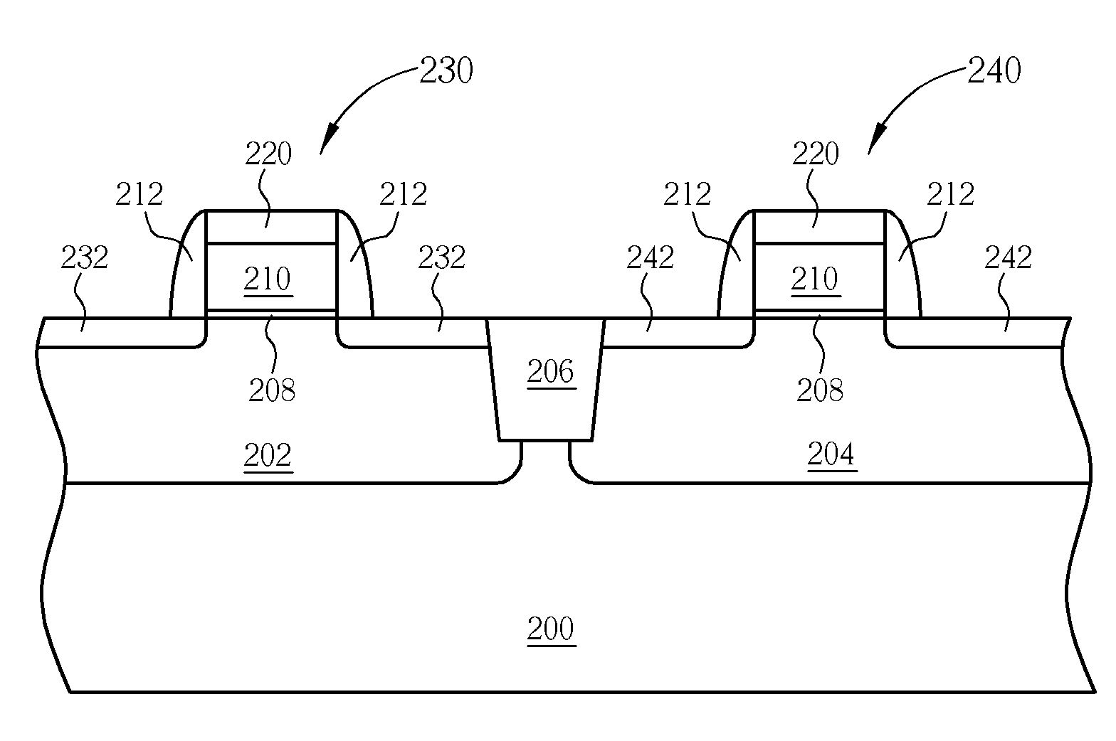
[0024]Please refer to FIGS. 7-12, which are schematic drawings illustrating a method for manufacturing CMOS transistors according to a first preferred embodiment. As shown in FIG. 7, a substrate 200 comprising a first active area such as a first type well 202, a second active area such as a second type well 204, and a shallow trench isolation (STI) 206 formed in between is firstly provided. Forming a first type gate structure 230 and a second type gate structure 240 respectively in the first type well 202 and the second type well 204. Each gate structure 230 and 240 comprises a gate dielectric layer 208, a gate conductive layer 210, and a hard mask layer 220 comprising silicon oxide (SiO2), silicon nitride (SiN), silicon oxynitride (SiON), silicon carbon nitride (SiCN), silicon carbide (SiC), silicon oxycarbide (SiOC), or silicon-rich-nitride (SRN). The hard mask layer 220 used to define a position of the gate conductive layer 210 and to protect the gate conductive layer 210 in foll...


PUM


Abstract

A method for manufacturing CMOS transistors includes an etching back process alternatively performed after the gate structure formation, the lightly doped drain formation, source / drain implantation, or SEG process to etch a hard mask layer covering and protecting a first type gate structure, and to reduce thickness deviation between the hard masks covering the first type gate structure and a second type gate structure. Therefore the damage to spacers, STIs, and the profile of the gate structures due to the thickness deviation is prevented.

Description

BACKGROUND OF THE INVENTION [0001]1. Field of the Invention[0002]The present invention relates to methods for manufacturing complementary metal oxide semiconductor (CMOS) transistors, and more particularly, to methods for manufacturing CMOS transistors with selective epitaxial growth (SEG).[0003]2. Description of the Prior Art[0004]As semiconductor processes advance to very deep sub-micron geometries and with the progress of device miniaturization, enhancing carrier mobility and a driving current of a MOS transistor has become a critical issue. For example, manufacturing source / drain of a MOS transistor with selective epitaxial growth (SEG) technology is used to improve electrical performance of those elements. SEG technology is widely applied in manufacturing numerous kinds of semiconductor devices, such as MOS transistors having raised source / drain region which benefits from good short channel character and low parasitical resistance and a MOS transistor having recessed source / dra...

Claims


Application Information

Patent Timeline
Patent Type & Authority Applications(United States)
IPC IPC(8): H01L21/8238
CPCH01L21/823814H01L21/823828H01L29/7833H01L29/165H01L29/66636H01L21/823864
Inventor LIANG, CHIA-WENHUANG, CHENG-TUNGTING, SHYH-FANNWU, CHIH-CHIANGHSU, SHIH-CHIEHJENG, LI-SHIANLEE, KUN-HSIENWU, MENG-YIHUNG, WEN-HANCHENG, TZYY-MING
Owner MARLIN SEMICON LTD
Why Eureka
Try Eureka