

Multi-channel error correction coder architecture using embedded memory
a coder and error correction technology, applied in error detection/correction, redundant data error correction, instruments, etc., can solve the problems of reducing the read performance in the memory system, requiring more detection and correction steps, and causing the error of reading data from the memory devi
- Summary
- Abstract
- Description
- Claims
- Application Information
AI Technical Summary
Problems solved by technology
Method used
Image

Examples
first embodiment
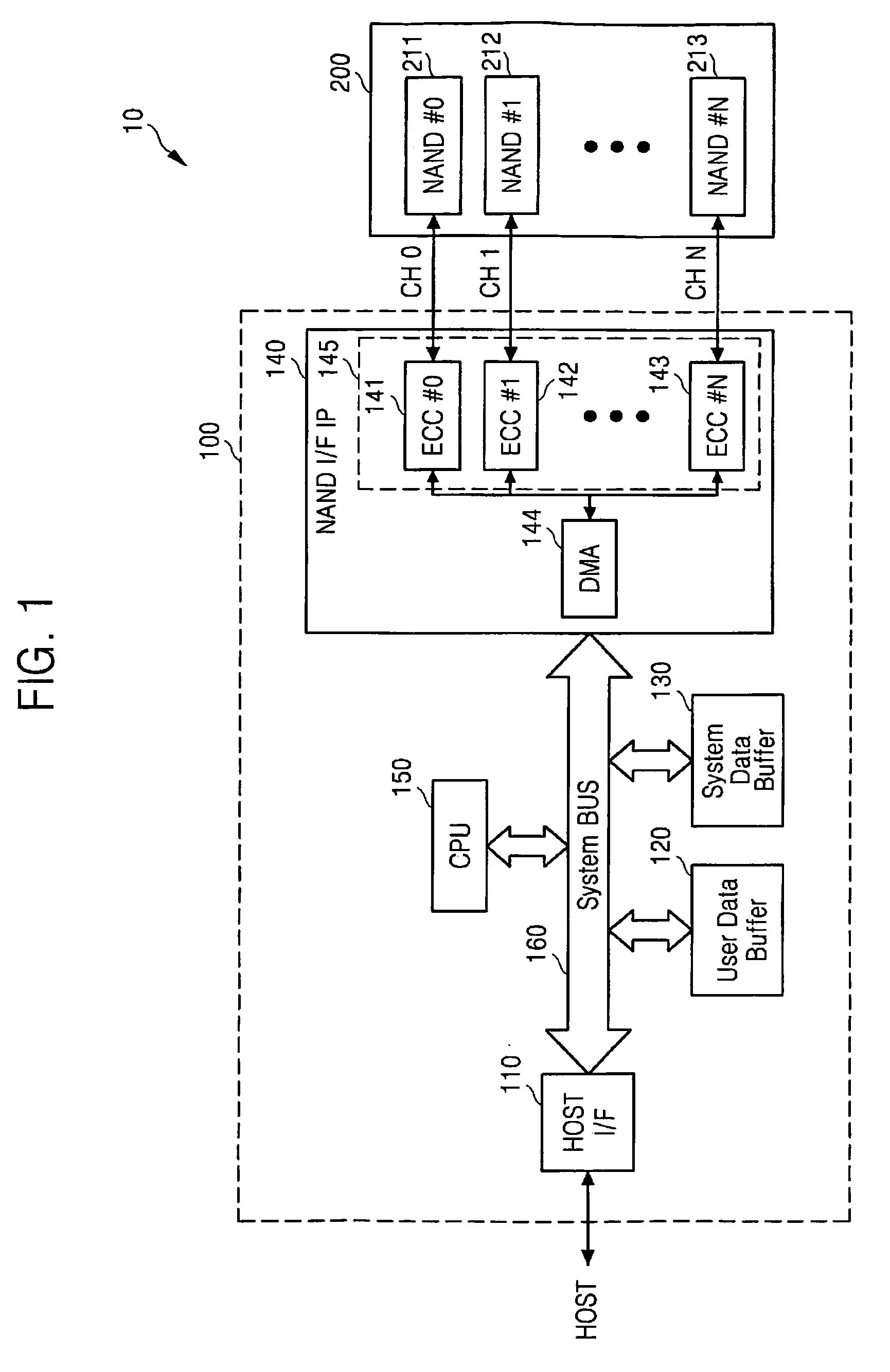
[0030]FIG. 4 illustrates a memory system 400 where error correction coder (ECC) is provided in internal buffer circuitry. Memory system 400 includes a flash memory controller 405 and a memory block having a plurality (N) of NAND memory devices, including memory devices 411 and 421 and other memory devices not shown in FIG. 4. Memory controller 405 includes a host interface 410 and buffers 420. Memory controller 405 also includes a NAND interface 440, and a central processing unit 450, an error correction coder (ECC) block 445 and internal static random access memory (SRAM) 430 all connected together by a system bus 460. NAND interface 440 includes a direct memory access (DMA) controller 444 connected to each of the memory devices 411, 421. etc. via corresponding communication channels as illustrated in FIG. 4.
[0031]FIG. 5 illustrates one embodiment of a buffer controller that may be included in the memory system of FIG. 4. As shown in FIG. 5, buffers 420 include buffers for user dat...
second embodiment
[0033]FIG. 6 illustrates a memory system 600 where an ECC is provided in internal buffer circuitry. Memory system 600 includes a flash memory controller 605 and a memory block having a plurality (N) of NAND memory devices, including memory devices 611 and 621 and other memory devices not shown in FIG. 6. Memory controller 605 includes a host interface 610 and an error correction coder (ECC) block 645. Memory controller 605 also includes a NAND interface 640, and a central processing unit 650, buffers 620 and a decoder 630 all connected together by a system bus 660. NAND interface 640 includes a direct memory access (DMA) controller 644 connected to each of the memory devices 611, 621, etc. via corresponding communication channels as illustrated in FIG. 6.
[0034]FIG. 7 illustrates one embodiment of a buffer controller that may be included in the memory system of FIG. 6. As shown in FIG. 7, encoder 645 encodes user data for multiple memory devices 611, 621, etc. and stores the encoded ...
third embodiment
[0037]FIG. 8 illustrates a memory system 800 where an ECC is provided in internal buffer circuitry. Memory system 800 includes a flash memory controller 805 and a memory block having a plurality (N) of NAND memory devices, including memory devices 811 and 821 and other memory devices not shown in FIG. 8. Memory controller 805 includes a host interface 810 and an error correction coder (ECC) block 845 (not shown in FIG. 8, but shown in FIG. 9). Memory controller 805 also includes a NAND interface 840, and a central processing unit 850, buffers 820 and a decoder 830 all connected together by a system bus 860. NAND interface 840 includes a direct memory access (DMA) controller 844 connected to each of the memory devices 811, 821, etc. via corresponding communication channels as illustrated in FIG. 8.
[0038]FIG. 9 illustrates one embodiment of a buffer controller that may be included in the memory system of FIG. 8. As shown in FIG. 9, encoder 845 stores encoded user data in buffers 820, ...
PUM
 Abstract
Description
Claims
Application Information