Semiconductor device

a technology of semiconductors and devices, applied in the direction of transistors, television systems, television system scanning details, etc., can solve the problems of junction capacitance and deterioration of switching characteristics

Active Publication Date: 2009-01-29
SEMICON COMPONENTS IND LLC
View PDF5 Cites 18 Cited by
  • Summary
  • Abstract
  • Description
  • Claims
  • Application Information

AI Technical Summary

Benefits of technology

[0019]The invention provides a semiconductor device that includes a semiconductor substrate of a first general conductivity type configured to operate as a back gate region, a channel region of a second general conductivity type disposed on the front surface of the semiconductor substrate, and a gate region of the first general conductivity type formed in the surface portion of the channel region so as to form a mesh pattern having first mesh cells and second mesh cells. Each of the first and second mesh

Problems solved by technology

Accordingly, an increase in the area of the box B leads to an increase in gate junction capacitance, an

Method used


Image

  • Semiconductor device
  • Semiconductor device
  • Semiconductor device

Examples


Embodiment Construction

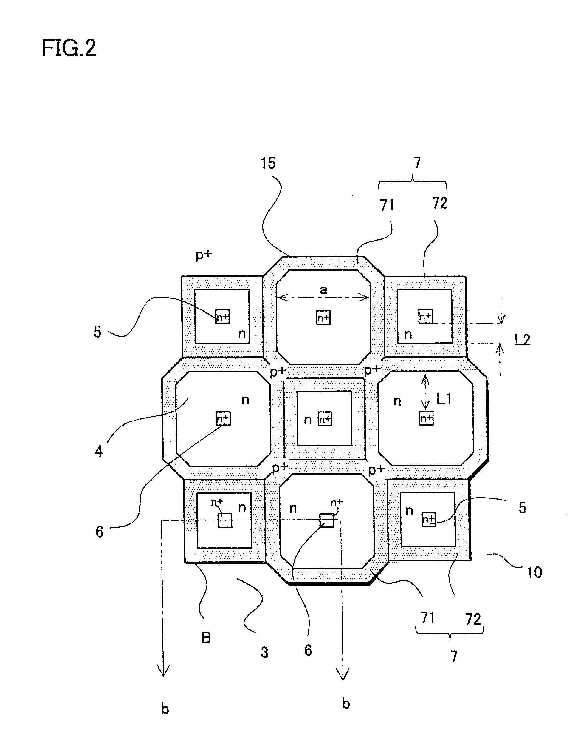
[0026]Hereinbelow, with reference to FIGS. 1 to 3, an embodiment of the invention will be described by using a junction field effect transistor (J-FET) as an example.

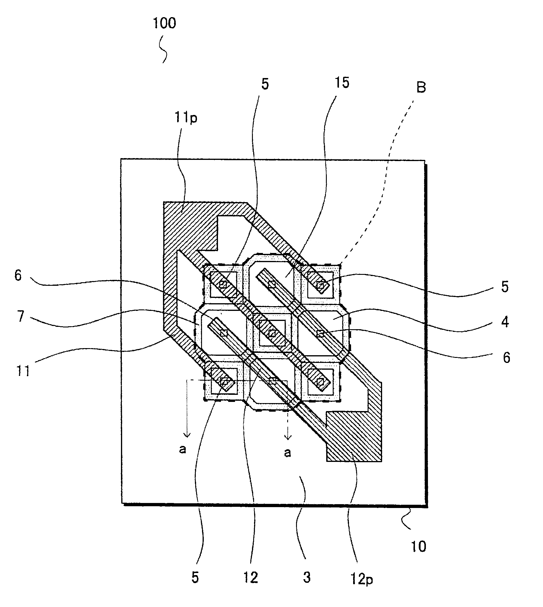
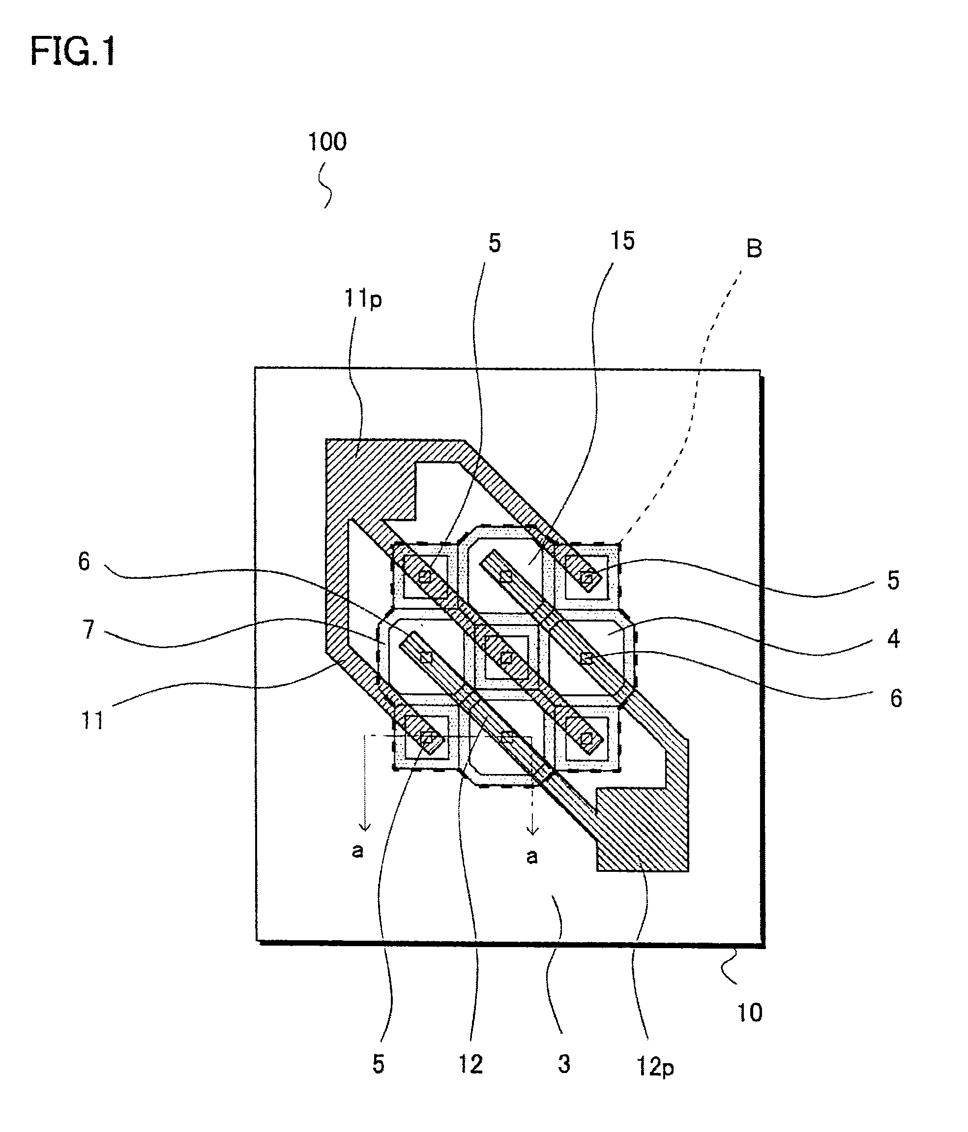
[0027]FIG. 1 is a plan view illustrating a J-FET 100 according to the embodiment.

[0028]The J-FET 100 according to this embodiment includes a semiconductor substrate 1 of one conductivity type, a channel region 4, a gate region 7, source regions 5, and drain regions 6.

[0029]The J-FET 100 has an active region 15 provided on the p type semiconductor substrate 1 forming a single chip, and serving as a back gate region. Here, although a single active region 15 is provided as an example, a plurality of active regions 15 may be provided.

[0030]The active region 15 collectively refers to the channel region 4, the gate region 7, the source regions 5, the drain regions 6, as well as source electrodes 11 and drain electrodes 12 provided on and connected to the source regions 5 and the drain regions 6, respectively. In this embodime...


PUM


Abstract

In the semiconductor device, a gate region is formed in a mesh pattern having first polygonal shapes and second polygonal shapes the area of which is smaller than that of the first polygonal shapes, and drain regions and source regions are disposed within the first polygonal shapes and the second polygonal shapes, respectively. With this configuration, the forward transfer admittance gm can be increased as compared with a structure in which gate regions are disposed in a stripe pattern. Furthermore, compared with a case in which a gate region is disposed in a grid pattern, deterioration in forward transfer characteristics (amplification characteristics) due to an increase in input capacitance Ciss can be minimized while a predetermined withstand voltage is maintained.

Description

[0001]This application claims priority from Japanese Patent Application Number JP 2007-195818 filed on Jul. 27, 2007, the content of which is incorporated herein by reference in its entirety.BACKGROUND OF THE INVENTION[0002]1. Field of the Invention[0003]The present invention relates to a semiconductor device used in a high frequency device, and particularly relates to a semiconductor device having a reduced chip size and improved high frequency characteristics.[0004]2. Description of the Related Art[0005]FIG. 4 illustrates an example of a junction field effect transistor (hereinafter, referred to as J-FET) used in high frequency devices.[0006]FIG. 4 is a plan view showing a J-FET 200. The J-FET 200 has active regions 35 provided on a semiconductor substrate 20 forming a semiconductor chip. The active regions 35 are isolated by an isolation region 23. In this example, the two active regions 35 are provided, and both have the same configuration.[0007]The active regions 35 each have t...

Claims


Application Information

Patent Timeline
IPC IPC(8): H01L27/098
CPCH01L29/0692H01L29/808H01L29/1066H01L29/80
Inventor MATSUMIYA, YOSHIAKIHATAMOTO, MITSUO
Owner SEMICON COMPONENTS IND LLC
Why Eureka
Try Eureka